Wednesday, May 22, 2013

How to export vector figures from MATLAB (or, the saddest thing is how elated I was when I finally figured this out)

Lately, I've been producing a lot of figures for my dissertation in MATLAB (my scientific computing platform of choice).  Once the figures are created, they need to be transferred into a word processor (e.g, Microsoft Word) to become part of my contribution to the advancement of science.

The problem is that this is a more complicated procedure than one might think.  The most straightforward method would be to save the figures as some sort of bitmap format (png, jpg, etc.); however, this means that the resolution is set and the figure labels, annotations, trace widths, etc. cannot be changed without going back to MATLAB, changing those things in the figure, then re-exporting it.  The alternative is to save the figure in a vector format; .eps would be ideal, but Word's support is spotty, so I use .emf.  A vector format saves a description of the shapes that make up the figure (lines, letters, patches of color) rather than a raster of pixels; this way, you can unpack the figure after-the-fact and change things in the word processor (line widths, fonts, labels) without having to go back to MATLAB.

The problem I had was that the vector images that MATLAB exported were... jagged.  Disjointed.  Weird.  Specifically, I need to plot EMG traces (ElectroMyoGrams, the electrical activity of muscles); some examples of this are shown immediately below.  The two figures immediately below are screenshots of the same data from within MATLAB; the left is just a zoomed-in subset of the right figure.  As you zoom in, MATLAB re-renders the image on the screen based on the actual data that was plotted.

Several traces of EMG, as seen natively in MATLAB
Zoom in of EMG traces, natively in MATLAB, showing normal spikiness of EMG
 The problem happened why I tried to export these figures into a vector format that I could insert into a Word document.  I first tried exporting as .eps; this did not work AT ALL.  When I exported to .emf, things appeared to work better (see the screenshot immediately below).  However, when zoomed in, the traces were 'jagged'.  Additionally, smoother traces (joint angles corresponding to the EMG) appeared 'quantized' far more than in the original figure.
Screenshot of exported figure in PowerPoint
Screenshot within Powerpoint of the figure above, zoomed in, showing 'jagged' trace
This was very confusing; why would the vectors be quantized? they represent the underlying data from the figure, right?  Searching online was largely in vain; the keyword 'jagged' was of no help, and most of what turned up was just generic 'how do I export MATLAB' how-tos.  After trying a series of progressively more esoteric and unnatural transformations (export to eps, open in ghostscript, export to emf, import into Powerpoint...), I finally found this thread on the MATLAB Central forum.  A few posts in, one person notes that "

 the resolution of the metafile is limited to screen resolution. This
means when we draw a line segment the endpoints are on a grid at screen
resolution. So even though the line is drawn at device resolution the
endpoints could be at a much lower resolution. This problem usually shows up
when you have lots of short line segments -- Ben Hinkle
AHA!  I had my answer.  The problem was not bad emf support in MATLAB or Powerpoint, but the fact that the default renderer creates the ends of the line segments in the vector image export at the resolution of the screen.  However, that post was from 2000, so MATLAB has advanced slightly since then; I was able to find an export setting that allowed me to force the resolution of the renderer to be higher than the screen resolution.

So, in the end, my MATLAB-to-Word (by way of Powerpoint for manipulation, because I am too cheap for Corel et. al) is:


  1. Create the figure in MATLAB
  2. In the MATLAB figure window, File -> Export Setup; under the Rendering tab, choose 'Painters' as the renderer (the other two are rasterizers) and 600 as your DPI (or 300 or 100, whatever floats your boat).  Presumably, 'Auto', which it was set to, had somewhat too-low standards for my needs.
  3. Apply to Figure
  4. Export -> set your file type as .emf.
  5. In Powerpoint, Insert -> Picture -> choose your figure
  6. Right click on the figure -> ungroup -> yes (this 'unpacks' the figure in Powerpoint, allowing you to manipulate the vector objects that make it up)
  7. Manipulate the figure, then directly copy/paste into Word (don't forget to re-group the figure elements before copying)

The end result is seen below; unfortunately, Powerpoint wouldn't let me zoom in any further, but it's clear that the figure as exported is far more faithful to the original than before the 600DPI setting.  Additionally, smoother traces no longer suffer from 'quantization'.


Thursday, March 7, 2013

Toward triangular-tesselated Game of Life wrapped onto regular polyhedra (or, MATLAB's handle graphics interface is simultaneously terrible and the best solution possible)

As I outlined in a previous post, I want to build a device which will display Conway's Game of Life.  To make things a little more interesting, it will do this using a triangular tesselation (rather than the much more common square pattern), and faces of 25 pixels will be folded and assembled to form a regular polyhedron.

Since building the device will be a large undertaking and the firmware will be very complicated (in a way which would make small errors generally difficult to isolate), I have implemented the device in simulation using the MATLAB environment.  This has allowed me to verify that my mapping of the pixels and implementation of the game update rules is correct.

Tetrahedron

The first shape is the tetrahedron, show below.  Since the tetrahedron is difficult to visualize in a 2D projection, I've posted two images of the same pattern from two different angles.  It's a period-3 oscillator under the rule {4,6,4,4}.  Implementing this form will only require one of the four-triangle circuit sets I've designed.

Octahedron

Below, I show show the evolution of a glider pattern, also under rule {4,6,4,4}.  The period of its circumnavigation of the device is 45.


Icosahedron

The same glider pattern, also rule {4,6,4,4}.  Circumnavigation takes 75 generations.


Source

The MATLAB files I used are here.  To instantiate one of the above forms, just run createIcosaTRI([4,6,4,4]), with your desired rule in the brackets.  The other shape creation functions are createTetraTRI and createOctaTRI.

Saturday, February 23, 2013

Initial validation of joint sensor glove board (or, at least I didn't put the USB jack in backwards this time)

As I related in a past post, I recently designed and built a device which could be built into a joint-sensor glove; it is able to measure the resistance of 25 sensors and store that data to a microSD card or stream it over a serial link.

I started this project because I've long wanted to play around with using an instrumented glove which would allow free-form hand gestures to be used as a human interface.  Additionally, I work with people who do research into physical rehab, who sometimes need access to hand movement data.  Currently, they have to use a bulky device which is wirelessly tethered to a PC; this restricts the circumstances under which data can be taken.  This device, being able to be contained in a glove and being able to store data internally, may allow for experiments which are not currently viable (e.g., a full-day recording to examine the structure of normal hand use).

Hardware

A front image of the board is below.  The front only has two buttons, two status LEDs, and the low-frequency, high-accuracy clock oscillator.


The back of the board is below.  The resistive sensors would be connected to the header at the top; the top row of holes all connect to +3.3V and the bottom row lead to the FET switch array.  Currently, I've got a potentiometer connected for first-round debugging.

The actual resistance-sensing circuitry uses a FET and an opamp to sink a set amount of current through the selected sensor channel.  The sensor channel is selected by turning ON the appropriate FETs in the line of ICs just below the sensor header at the top; it is a 5-by-5 array, allowing one of 25 sensors to be selected by the appropriate use of 10 outputs.  The voltage at the bottom of this switch array is sampled to measure the resistance; since the current sink is controlled, the voltage difference between 3.3V and the measured voltage determines the resistance.

The board also includes the microSD slot (bottom left) and the power circuitry (charger and 3.3V buck converter, bottom right).  All of the circuitry has been tested except the microSD slot.


Software + Testing

To start testing the hardware, I developed a simple firmware which will sample the 25 sensors and transmit the resulting voltages over the serial channel that I have broken out for debugging.  The firmware source is here; it is very simple, and applies a constant sink current across all of the sensors and over time.  In the future, it may make sense to adjust the sink current to match the sensitivity and range of the device to the magnitude and range of resistances exhibited by each channel.

The firmware sets the switch array and samples each 'sensor' in turn; the data is then partitioned and inserted into a transmit buffer.  Once all of the channels have been sampled, I use the DMA controller to 'automatically' transmit the buffer contents over the serial link.

To watch the data as it comes in, I use an upgraded version of my general-purpose MATLAB serial data 'scope function (here).  First, I verified that all of the channels were working by shorting each channel in turn (shown below); as you can see, all of the channels were working.


I then wiggled the potentiometer at either end of its range, to cause wiggles in the scope for the appropriate channels (below).


This means that, with the exception of the SD card slot, all of the hardware has been tested and verified.

Moving Forward

Since I know that the resistance sensor circuit works (in a broad sense), there are a number of things to do:

-Implement the SD-card logging.  This will involve testing out the hardware and its ability to interface with SD cards, looking up the specs for SD card partitioning and FAT32, and using that information to implement some simple code that finds a long stretch of unused space on the card to fill up with logged sensor data.  It would be possible to code something that does not require a contiguous segment of the drive; however, this would require a much more complicated algorithm.  Since this is a very purpose-built device, that seems like overkill; one merely needs to make sure that the SD cards used are relatively empty and absolutely defragmented.

-Implement a limited USB serial port.  At present, the hardware is able to communicate over USB (verified by flashing the device with a USB-based bootloader).  However, I do not use this facility; further, to get debug or other data out of my prototypes, I use a separate USB-to-serial cable connected to a debug USART.  This extra cable is somewhat cumbersome; it would be nice to only need to plug in one cable to power the device and allow for debugging and reprogramming.

-Make an example resistive joint sensor; develop the algorithms to read it.  At present, I just set the sensor current sink to a constant level.  However, for certain ranges of resistances to-be-measured, it will saturate, while others will barely register.  Additionally, an increase in resolution may be possible by sampling the sensor output single-ended, then also sampling it differentially with a bias input set equal-ish to the single-ended value.

-Make a glove; fill it with joint sensors.  Obviously, I eventually need to actually make a glove to sew sensors into, and then connect to the device.

Migration to sleep mask v2 (or, the device now lacerates the user's face in only 12% of use cases)

So, I finally got the hardware for the second version of the sleep mask to work.  Turns out, if your firmware waits for the real-time clock to stabilize the external crystal oscillator, it helps to have one attached.

The device front and back are pictured below; it is running on its own power, and all of the main subsystems are working.


Of course, I forgot to add a line from the battery to the ADC to allow for charge status to be monitored; that's one definite change for V3.

Moving forward, I need to:

-Take a few nights' worth of data, to make sure that the REM detector still works
-Develop a filter/classifier to determine whether REM was happening based on the detector output.
-Assess power usage again, and implement the lowpass in front of the headphone amplifier to see if that reduces power use.
-See what's going on with the headphone detection circuit; I cribbed this from an application note, and it was implied that it would just give a digital output; this has not been the case.

After the classifier is determined, I'll start to design the overall structure of the working firmware; it'll have to take into account the needs of the REM classifier and the headphone noise generator while also keeping track of current time, alarms and current and past REM states.


Friday, February 22, 2013

First steps for unnecessarily complicated paperweight (or, inconsequential blinking-light projects evolved)

For a long time, I've wanted to make a project that implemented Conway's Game of Life in electronics, as a kind of creating-for-its-own-sake thing.  The Game of Life (GoL) is a program that computes the 'evolution' of a population of cells on a square, 2-D plane.  It has some interesting computational properties, but I was mostly interested in it because, when observed over time, the cells have a kind of ordered chaos aesthetic.

My original yen (more than a decade ago) was to just build a HUGE matrix of LEDs and use them to display  the ongoing evolution via GoL of a random starting seed state.  However, this is A) expensive, in both space and currency; and B) not novel any more.  There have been a number of physical GoL implementations; in fact, you can buy a kit for a four-by-four matrix which can be tiled with other kits to make an arbitrarily large GoL implementation.

Playing around with the idea, I recently decided to make something out of the GoL with a triangular tessellation, rather then the usual square grid.  Fortunately, there was some literature on this subject (Bays, Carter. Cellular Automata in the Triangular Tesselation. Complex Systems 8 (1994) 127-150), so I didn't have to reinvent the wheel; additionally, his work specified which GoL rules would lead to interesting behavior.  He also discovered several glider patterns, so that I could incorporate them into non-random, pre-specified seed states if I so wanted.

I made a quick-and-dirty triangular tessellation display, as seen in the video below; I hooked it up to an ATXMEGA32A4U with a firmware that would start with a pattern, then allow it to evolve over time until there are no cells left, at which point it would reset to the original test state.


My goal was to create independent 5-by-5 triangular units which could be used as the faces of an icosahedron.  However, this ended up requiring a LOT of microcontrollers and a LOT of by-hand jumper soldering, owing to difficulties in routing one tiny board with a big microcontroller on one side.  I've since settled on a design which uses one microcontroller per four faces; this made the routing easier (in only have to solder the edges of the triangles together, with on jumpers) and significantly reduced the overall project cost, since I would only need five microcontrollers instead of 20.

At present, I have the set of boards for the matched four triangular faces designed, and the bill of materials for the faces set.  I just need to double-check those boards, design the power supply circuitry for the center of the icosahedron, add a board for V2 of the turn signal gloves, finish my doctoral thesis, sit for the USPTO registration examination and start my new job.  i expect to resume work on this project sometime after Labor Day.  2014.

Sunday, December 16, 2012

Replacing the middle button on the Logitech M570 Wireless Trackball (or, yes, I really do love this trackball that much)

I've been using a wireless trackball for a while now, and it's turned out to be one of the best purchases I've ever made.  It's especially excellent for working on the train, since i don't like the trackpad and there isn't room for a normal mouse.

The wireless trackball I'm using is the Logitech M570.  It has a combination scroll wheel/middle button; however, over time this button began to get flaky.  There would be weeks where the button wouldn't respond at all, or would only respond to exceptional force. Looking online, this seems to be a common problem; the device is somewhat cheaply made, and the middle button is not the usual high-performance switch, but some lower-quality part.

I set out to determine whether the button could be replaced; I was successful, and my procedure for replacing it is outlined below.  The new button is slightly stiffer than the old, but it works consistently.

Button Replacement Procedure

Disassembly

First, pop the blue trackball out.  Then, there are five screws holding the shell together; remove them.  Note that one of these screws is beneath the sticker in the battery compartment (shown below).


With the shell off, you'll need to remove the circuit boards.  First, detach the ribbon cable leading to the trackball reader (the gold bit in the middle of the image below); to do this, you'll have to pull up the plastic locking connector.  Then, remove the four screws which keep the circuit boards on the lower shell, and pick up the circuit board assembly.  Take care not to bend the battery wires as you remove them from the lower shell.  The middle/scroll wheel button we're going to replace is just in front of the ribbon cable.


Old Button Removal

In removing the old button, we need to be careful not to damage the rest of the circuitry.  Note that our task is made easier by the fact that we don't care what state the old button ends up in.  The method I used to avoid damage to the surrounding circuit is shown below; first, I used a diagonal cutter to cut the two forward leads on the button.  Once this was done, I gently rocked the button up and down to weaken and then break the remaining two leads of the button and remove it (I did not cut these leads, as there were difficult to access without risking damage to the rest of the circuit).


Once the button is mostly removed, I used copper solder wick to clean up the four holes that the leads of the button formerly inhabited.

New Button modification and installation

If you were paying close attention during the old button removal, you'll notice that the leads were pretty much vertical.  The buttons I had on hand were very similar in size and function (normally open, leads paired length-wise); however, their leads were gull-wing SMD style (MOUSER link).  Before I can install it, I need to manipulate the leads into a more vertical configuration, detailed in pictures below.


First, push the leads down.


Then, use pliers to straighten the leads downward.


Then, gently insert the button into the cleared holes and solder it into place; be sure that it is flush with the surface of the circuit board.


Re-Assembly

Just reverse the steps in Disassembly.  It is important to make sure that the little plastic power button in the lower shell is lined up with the switch on the circuit board before screwing everything back together (the switch is the silver-and-black affair on the lower right of the picture above, just in front of where the battery clips attach to the circuit board).


It is interesting to note that Logitech uses Nordic Semiconductor radios for their wireless links (at least for the new-ish unified receiver).

Tuesday, December 11, 2012

My initial investigation of the MARLOK key (or, how many times do I have to mess up using a pipelined ADC before I'll learn my lesson permanently?)

As I mentioned in the previous post, my university uses a somewhat rare access control technology called 'MARLOK': each user is issued a key, whose identity is encoded in a series of holes in the shank of the key (kind of like an old punch-card).  The key is inserted into a reader next to a door, and if the user has privileges to the door, it is momentarily unlocked.

I was interested in reading the key (and possibly eventually building something to emulate the key, in a reader), so I had a couple of little boards made to mount infrared emitters and detectors at the appropriate distances to read the three tracks of the key.

Initial Research

Before doing all this, I tried to look up the MARLOK system on the internet.  Details were sparse; the only information of any substance is here, where someone reports that each key encodes 24 bits of ID.  Otherwise, there's very little info out there; nothing on the structure of the encoding, how the clock is embedded/recovered, etc.

The Current Test

The sensor (with key inserted) is shown below.  The emitters are Kignbright APT2012F3C; they are wired in parallel with a 460Ohm current limiting resistor, leading to a total of 5mA passing through them collectively.  The detectors are Everlight PT19-21C/L41/TR8 phototransistors; they are connected to the positive rail, and then through 2.2kOhm resistors to ground.  The voltage is sampled at the top of the resistors by a microcontroller, then sent out at 100Hz through the serial port.

The key has three tracks; the black plastic is infrared-transparent.  The metal of the key is punched with square holes to allow for IR light to travel through the key.


The ends of two of the tracks were totally accidentally exposed, to show the structure of the holes (shown below).  As you can see, the holes are square.  From the data I show later, the middle track is a clock signal; this makes sense, as the middle hole is offset from the exposed side track by a half-hole-width, so that transition on the clock track signals when to sample the data tracks.


Below is a plot of the three track traces; the left is when the sensor was seated at the base of the key, and the right occurred as I slid the sensor off the key.  Green is the middle track, red and blue are the side tracks.  Note that it took a little messing around to get this data; originally, the LED current was three times what it was for these trials, and it saturated the clock channel (since, being in the middle, it got illumination from all three LEDs).


This next is the same information, but at the end of the sensor removal, as the sensor comes of the end of the key.


From the data, I saw that the middle track was the only one that was always on; from this (and the fact that its holes were offset from the other tracks' holes), I assume it is the clock signal.

Looking at the traces over a full sensor-removal, I saw the following patterns of holes:

01111110011101
11111111111111 END OF KEY>>
00001001110111
As i said above, the middle track was the only one that was always 'on'.  Additionally, since the first clock has both 'on', and the last has both 'off', and the internet says these keys encode 24 bits, and there are 14 total clock pulses, I assume that the end-of-key data track bits are always 'on', and the base-of-key data track bits are always 'off', which likely helps in level determination and data recovery.

Moving Forward

As evidenced in the data traces, I'm having difficulty keeping the key straight in the sensor; I'll need to do something to mechanically narrow the passage.  Once this is done, it'll be possible to recover sampling times from the clock transitions.  It might also be possible to improve the signal level by masking the LEDs so that they don't bleed over into the other channels as much.

Data Recording Software

To get this data, I created a microcontroller firmware that samples the three channels, then packs each 12bit sample into a message packet (which includes a start sentinel nibble for frame alignment) and sends it over the serial port.  I then created a general-purpose serial port data-extractor and -viewer for MATLAB, which is available here.

Thursday, December 6, 2012

Final bugs and V2 (or, yes, I actually labeled the USB pins in reverse order. Stop laughing)

I've finally figured out what was wrong with the sleep mask charger and USB circuits: the pins on the connector were reversed.  So, hilariously, every time I plugged it in, i was connecting V+ and GND backwards, leading to some considerable heating in the charger IC.  Remarkably, the whole thing worked flawlessly once I flipped the connector.

Since I worked that out, I've designed version 2 of the sleep mask and helmet boards.  Additionally, I designed boards for a few other projects, including an instrumented glove, and MARLOK key reader and a pulse oximeter.  I've begun to populate the boards, but I'm out of some things, so I'm waiting for another Mouser order.  Unfortunately, the component names ended up on the silkscreen, making it thoroughly messy.

Sleep Mask V2

After figuring out what I'd done wrong with the USB connector (as well as playing around with the REM detector), I moved forward with redesigning the sleep mask controller board.  Most importantly, I significantly shrunk the board (the old version was very... clunky).  I used smaller versions of the microcontroller, FET, headphone jack and opamp.  Additionally, I added the option for a lowpass between the microcontroller DACs and the headphone amplifier, in the hopes that I can reduce power consumption.


I also wired up a new mask (the old one was... clunky.  Also gaudy... very gaudy).


Helmet V2

The new version of the helmet implemented the analog-power-off changes, in addition to adding a charger circuit.  However, it ends up being about the same size of the old board, owing to the use of smaller FET, opamp and microcontroller.


Instrumented Glove

I've long been interested in the idea of a joint-angle-sensing glove for computer interface.  Additionally, I overheard someone around the lab implying that they would like to take such joint data over a whole day of normal hand-use.  So, I thought that I could use some of the spare board-space on a circuit which would read at least 22 channels of joint angle data, and record them to an SD card.  The flex sensors will be home-made, and will change their resistance with flexion (like in this article).

I decided to go for a controlled-current topology for resistor-sensing (rather than a divider) to get a linear read on the resistance.  The resistor sensors are connected to the header at the top of the board; they connect to V+ on one side, and to the constant-current sink on the other side, through a matrix of FET switches; 5 banks of 5 sensors each give me 25 potential sensor channels for a mere 10 digital outputs.  This circuit also includes a battery charger.


MARLOK key reader

I've long hated the MARLOK key; it seems like a perfect storm of high-cost and low-convenience and I don't understand why you would use it instead of an iButton system or RFID.  In any event, I have a MARLOK key and I was curious about how the information (and clock) were encoded in it.  There isn't much information online about the format; all I was able to find was that the information is encoded in the sequence of holes drilled in the shaft of the key.

I designed a pair of board upon which I could mount IR emitters and IR phototransistors to read all three tracks of the key; I added a few spare holes to weld the two sides together using wire scraps.


Pulse Oximeter Sensor

Finally, I wanted to try out reading pulse (and possibly blood oxygenation) non-invasively.  I created a sensor board based on "A wireless reflectance pulse oximeter with digital baseline control for unfiltered photoplethysmograms" by Kejia Li and Steve Warren.  The sensor is reflectance-mode, which means that you only need access to the surface of the body; in opposition to the transmission mode, where the emitter is opposite a protruding bit of anatomy (like a finger) from the detector.  The emitters and detectors are in the upcoming order, so it's just the board and cable for now.


Thursday, October 25, 2012

REM detector + display updates (or, scrolling displays are almost as cool as fezzes)

As I remarked in a recent post, I've nailed down the cause of my pesky REM detector noise issue.  Additionally, I started sprucing up the display subsystem, using a DMA channel to significantly reduce the processor load needed.  I've taken another couple of steps forward, in that I've implemented a fix to the REM noise issue, and I've refined the display subsystem so that it can easily produce text and primitive graphics; these refinements are shown immediately below.

The bottom 3/4 of the display is the REM differential signal level, scrolling from left to right.  The numbers on top are the 32-bit integer holding the device's seconds counter (left) and the IR illuimnator level (right).

Not very interested waveform-wise, but a clearer picture.


The video shows the scrolling display in action; since the sensor is pointed at the couch arm, there's not much going on, except when I rotate it.

Implementation details, vaguely

On the display side, this is really only a slight complication of what I outlined previously; there's a local buffer that I draw on, and periodically I set the DMA channel to transmit the contents of that buffer to the display via the serial transmitter peripheral.  There's a little bit of trickery translating the signed ADC inputs into the bytes that get painted into the display buffer, but it's overall quite straightforward.  A zipped archive of the project files is here.

On the REM detector side, I'd determined that the reason I was getting 'bias noise' every four samples was that the PWM switching transients were making it into the ADC signal, and because the PWM and REM counters were not integer multiples of each other, they would only 'line up' every four samples.  To rectify this scenario, I modified the code to make sure that the sample timer is always set up to be an integer multiple of the PWM timer period.  I also set up the clocking of the timers to go through the XMEGA's event system, so that I could keep the timers in sync.  A plot of the signal below shows no abnormal patterns in the noise, so I think this has taken care of the problem.


Moving Forward again

So, my next step has to be nailing down the REM detector.  Specifically, I'm going to slightly modify the hardware so that I can quarter the PWM duty cycle.  This way, I can maximize the settling time between the PWM switching time and the ADC sample time.  After this is done, I'm going to assess whether this has had the effect of decreasing the noise; either way, I'm going to collect some real-life sleep data, and get cracking on whether I can assemble a filter/classifier that can detect REM.

Of course, this completely avoids the issue of the busted charger circuit; unfortunately, I still haven't secured access to a hot-air rework station...

Wednesday, October 24, 2012

Using DMA to automatically transfer display data (or, it's RTFM, not 'Haphazardly Cast Your Eyes Left to Right Over The Manual While Thinking of Something Else')

As an aside from the process of perfecting the REM detector, I decided to start to clean up the display-painting parts of the firmware.

It takes half a kilobyte of data to completely fill the display (128-by-32 off-or-on pixels) and the data is sent through one of the chip's serial peripherals.  Since there is so much data to transmit per display update, it takes a LOT of processor cycles to do so; it takes even more cycles to do so by waiting and polling the serial peripheral instead of setting up an interrupt (as I did to debug the display).

Since the process of getting that data out to the display could be fairly straightforward, it seemed like the perfect excuse to take advantage of the AVR XMEGA microcontroller's onboard DMA feature.  And since I made a couple of errors along the way (and couldn't find a straightforward explanation of my problem online), it seemed appropriate to describe the situation here.

What is DMA?

Briefly, DMA (direct memory access) is a way of taking the load off of the processor by 'automating' data transfers.  Specifically, the DMA controller transfers a block of data from one location in memory to another while the processor executes other tasks.  Without a DMA controller, any large data transfer would take up processor time as the processor accessed and copied each byte of data individually.

There are many situations where you would want to transfer a lot of data from one location to another, or a small amount of data from (or to) one location a great many times.  In my scenario, I have a buffer in local memory that represents what the display will look like; the buffer is local so that manipulating it (compositing the image, blanking regions, adding text) is easier.  However, that buffer data needs to be periodically sent (serially) to the display hardware.  Ideally, the DMA will automate the process of taking each byte of the buffer in turn and sending it to the serial peripheral when it's ready to accept the bytes.

Implementation on the XMEGA

The XMEGA A microcontroller that I'm using has four independent DMA channels.  Each of them has a lot of configuration, including the ability to specify the source and destination data addresses and the ability to set what triggers the data transfers.

My problem was that I didn't read the manual closely enough; I thought that setting the channel trigger to the serial peripheral meant that every time the send register was empty (the trigger source), that a single byte would be sent.  In the default mode, however, the trigger causes the DMA to transfer an entire block of data as quickly as possible; since the serial peripheral sends out bytes a LOT slower than the rate that the DMA controller pushes bytes, this meant that each transfer only resulted in a few randomly-selected bytes of the buffer actually being sent to the display.  This caused me some consternation until I re-read the manual and realized my error; this fast operation is useful when copying data into SRAM or other fast destinations, but completely inappropriate for slow, single-byte destinations like the USART peripheral.

For slower destinations which will need to signal the transmission of each byte (or each burst of 2, 4, or 8 bytes) one at a time, the 'Single-Shot Data transfer' mode is used.  This mode completes a single burst, instead of a whole block, with each DMA channel trigger activation.

Since I want to transfer the complete contents of the display buffer to a single address on the serial peripheral, I need the destination address to be fixed and the source address to increment during the transmission, and reset at the end for the next update.

The actual C code I used to initialize the DMA controller and channel on the ATXMEGA128A4U is shown below; USARTC1 is the serial peripheral I'm using as my transmitter (it's been set up in master SPI mode for my display module, and then used to initialize the display module) and debugBuffer is the 512-byte-long stretch of internal memory that I'm using as my display buffer.

//set up a DMA channel
//enable the DMA controller
DMA_CTRL = DMA_ENABLE_bm;
//set the burst length to 1 byte
DMA_CH0_CTRLA = ( DMA_CH_SINGLE_bm | DMA_CH_BURSTLEN_1BYTE_gc );
//set the following: source address incremented, reload after each block; destination address fixed (reload after each block)
DMA_CH0_ADDRCTRL = ( DMA_CH_SRCRELOAD_TRANSACTION_gc | DMA_CH_SRCDIR_INC_gc | DMA_CH_DESTRELOAD_TRANSACTION_gc | DMA_CH_DESTDIR_FIXED_gc );
//now set the DMA trigger source to the USART data register being empty
DMA_CH0_TRIGSRC = DMA_CH_TRIGSRC_USARTC1_DRE_gc;
//load the block transfer count register with the number of bytes in our blocks (that is, 128*4 = 512)
DMA_CH0_TRFCNT = 512;
//now put in the initial source address; should be the memory address of the first byte of the display buffer
DMA_CH0_SRCADDR0 = ( (uint16_t) debugBuffer >> 0 ) & 0xFF;
DMA_CH0_SRCADDR1 = ( (uint16_t) debugBuffer >> 8 ) & 0xFF;
DMA_CH0_SRCADDR2 = 0x00;
//now specify the destination address; the transmit register of the USARTC1
DMA_CH0_DESTADDR0 = (( (uint16_t) &USARTC1_DATA ) >> 0) & 0xFF;
DMA_CH0_DESTADDR1 = (( (uint16_t) &USARTC1_DATA ) >> 8) & 0xFF;
DMA_CH0_DESTADDR2 = 0x00;

Once the DMA channel is set up (and assuming the USART and display have been initialized), I can update the display with the current contents of the buffer by simply enabling the DMA channel:

DMA_CH0_CTRLA |= 0b10000000;

Thursday, October 11, 2012

Project Updates (or, I am probably not dead)

So, it recently came to my attention that I haven't posted in several months.  This is due, in large part, to my actually getting work done on my PhD.  This is also due to the fact that the next steps are relatively... un-glamorous and un-postable.  Specifically, I have a small issue with the REM detector, and I need to figure out what's wrong with the battery charger circuit.  On the up side, I was able to significantly reduce the standby power consumption of my helmet flasher so... little victories.

Charger Debugging

As it stands, the Lithium-Polymer battery charging circuit does not work.  This is ironic, as it was the only sub-circuit that I did not mock up and test before ordering the circuit boards (I even mocked up the 3.3V buck converter, which only had three components).  I did this because, well... I was just using the reference implementation.  I've gone over the design (and the physical artifact's correspondence to it) with a fine-toothed comb; at this point, I'd like to swap the chip to see if that's the issue.  Unfortunately, I do not own a hot-air rework station, so that is easier said than done.  Additionally, the chip gets REALLY hot and sources a bunch of current when you plug it in, which complicates debugging, as I can only leave it plugged in for short periods.  Further, even if I could simply replace the chip, I'd be leery of doing it, as the new chip could easily fry as well.  This is triply annoying, as I would like to add the charger to my helmet and run signal glove in their next iteration, but can't do that until I know I've got the circuit right.

REM Detector Hiccups

The specific problem with the detector is that, for certain levels of illumination, the the detector output follows a 'negative bias' for every fourth sample; this is illustrated below.  Looking at the 'noise' and mean of the signal after separating it into four down-sampled signals (that is, the first sub-signal is every four samples of the original, starting with the first sample of the whole record; the second is every four starting with the second, etc.), it appears that this really is just a constant 'bias' term added only to every fourth sample.
This is an example of the detector output against my hand; green is the differential signal, dark blue is the single-ended signal, and light blue/cyan is the illuminator amplitude.  As you can see, the signal appears to get much more 'noisy' as the illumination level increases, until it abruptly decreases at a certain level.
Zoomed in view of the 'noisy' segment from above; we see that the extra 'noise' is due to every fourth sample being much lower than the other three.  This pattern is also borne out in the single-ended signal.
My current hypothesis is that this is due to my use of low-passed PWM outputs to give myself some extra low-bandwidth analog outputs to control the REM detector illumination level and the differential signal bias level.  Specifically, since the sample-specific noise only occurs at certain levels of illumination, and then suddenly stops once the level raises above that level, I am lead to believe that it's something to do with the PWM switching time lining up with the ADC sampling time.

If that's the case, I'll have to decrease the passing of switching transients by reducing the corner frequency of the low-pass and/or increasing the carrier frequency of the PWM.  Of course, increasing the carrier frequency will reduce the resolution of the LP-PWM channels; however, since I don't use the full resolution anyway, it wouldn't be much of a sacrifice.

Helmet flash controller standby power reduction

Going back to the helmet flasher project, I noticed that the AA batteries were getting drained in a manner that was less-than-consistent with usage.  I recalled that I had been less than diligent in regards to standby power usage, so I figured I could shave off a few milliamps by taking a closer look.

There were two main methods I figured I could use to reduce standby power use: put the controller into a deeper sleep state while in standby, and modify the hardware so that I could remove power from the op-amps used int he constant-current LED drivers.

The first approach, going into a deeper sleep state, was the first I implemented since it didn't involve modifying the hardware.  Before making my changes, I inserted a 1-Ohm 1% precision resistor to measure the standby current draw.  I set the device to go into "power down" when going into the standby state, with wake-up accomplished by state change on any of the buttons.  Additionally, I set the device to go into "standby" while the timers count and wait to move on to the next flasher state.  The source is available here, in case it is useful to someone wanting to see how a non-human primate would implement the preceding.

After implementing the sleep state changes, the standby power consumption went from 2.1mA to 1.7mA.  Good, but we're not finished.  Since the on-state power consumption is in the range of 100-200mA, it was impossible to detect if my changes had an effect on on-state power consumption.

The next step was to switch off the power to the linear constant-current LED driver block.  The op-amps used in that block draw current even when the LEDs are off, so it made sense to try to switch the power off when the device was in standby.  Since the analog block was currently fed directly from the power rail, it was necessary to cut that source first.

Since the op-amps only draw a few milliamps (far less than the 30mA the controller pins are rated for), it made sense to feed them from one of the controllers output pins; this way, I didn't need to add any additional FETs.  After doing this, and making the appropriate changes in the firmware, the standby power consumption fell from 1.7mA to less than 0.1mA.

Overall, these changes reduced standby power consumption from 2.1 to 0.1mA; a more than 95% reduction.  This makes me much more comfortable with leaving the batteries in when I'm not using it.

Next Steps

So, the most immediate next steps involve fixing the REM detector problem outlined above and making the charger circuit work.  After that, though, there are a couple of immediate next steps:

Finally finalize the sleep mask hardware

The current version of the sleep mask hardware is... clunky.  Pointy.  Eye-pokey, even.  Since it was a first prototype, I didn't put all the effort in the world into optimizing the layout, or the parts (I just used the components I had on hand, instead of sourcing the absolute smallest I could find).  Once I'm confident that the hardware is up to snuff, I can source the absolute smallest components (especially the controller and FETs/op-amps and the passives) and re-design the board.  To do that, though, I need to rectify the problems listed above (REM four-sample noise, charger broken).  Additionally, I'll need to take a few nights' worth of data and specify a classifier/filter that can detect 'REM' to my satisfaction; if the hardware needs revision to get to that point, I'd rather do so before the next hardware revision.

On a somewhat unrelated point, I'm going to hack up the headphone amplifier hardware to see if I can't make it more efficient.  As it stands, the white noise component consumes the lion's share of the power for the device.  Looking at the output of the headphone amp, the 'square edges' of the DAC output are preserved to the output; this might be causing greater power consumption than necessary.  If I introduce a high-pass before the headphone amp and shave those square edges off, I might be able to significantly reduce my power consumption.

Update the helmet flasher and glove turn signal hardware; make a decision about the helmet

As I've said above, I'd like to make the turn signal glove and helmet flasher run on rechargeable lithium-polymer batteries.  To do that, I need to make sure that the charger chip and circuit work as advertised.

Additionally, I need to make some decisions about the helmet flasher.  As it stands, it steps the battery voltage up to 16V to drive the LEDs in series.  This was done partially since I originally had intended to add some EL wire to the helmet; EL wire requires ~150V AC, and my intent was to switch current through some step-up transformers.  The transformers could be smaller/have a lower turns ratio if my switched DC voltage was larger.

This step-up is expensive (3$ for the controller alone, to say nothing of the related caps and inductor).  However, the series wiring of the LEDs allows the brightness/current of the LEDs to be more consistent.  Maintaining the step-up would also mean that I wouldn't have to re-wire my existing helmet.

Design the sleep mask PCB version 2

As I said above, once the sleep mask hardware is finalized, I'll source smaller components, and then redesign to the circuit board.  I figure it will be installed above the nose in the mask, with leads going down to the REM detector and red LEDs.  I'll also incorporate power control of the analog block, as I did for the helmet above, to reduce standby power consumption.

Order new boards + components; assemble + test

Just what it says: pick the new smaller components, order them and the boards, then build everything.

Software development of the sleep mask

At this point, the hardware for the sleep mask should be more-or-less finalized.  All that will be left is putting together the firmware.

I haven't given a lot of thought to the design of the interface or the overall design of the firmware.  However, I have given some thought to potential features I can try out, including:
  • REM-relative wake-up alarm: only wakes you up if you are at the tail end of an REM cycle (or you've reached some no-later-then-this time).  I haven't checked the science behind this, but I've heard that you wake up more refreshed if you wake up at the end of a cycle, rather than during the deep sleep in the middle.
  • Sleep induction using entrainment: again, I haven't looked into how rigorous the science is behind this is, but some advocate the use of binaural beats or isochronous pulses to induce lower-frequency EEG states, assisting the user away from consciousness.
  • External cues for lucid dreaming induction: the original purpose.
  • Slowly increasing LED illumination to ease wake-up: just what I said, improve wake-up by gradually increasing illumination within the mask along with the natural dawn.
  • REM logging: save the timestamps of REM periods, allow them to be transferred over USB.  Share on facebook?
  • USB bootloader: I know that Atmel provides one, I just need to see where it's hosted and play with it.


Sunday, July 29, 2012

Bicycle helmet complete (or, the afore-promised inconsequential blinking-light projects)

I have finally completed the bicycle helmet flasher project (that I added as an afterthought to the REM sleep mask PCB).  The design and fabrication of the controller module was outlined in a previous post; here I show the results of finally installing the lights into my existing helmet.


Additionally, the source has been slightly modified (available here); the device now has three buttons, one each for brightness of the forward and rear lights and the third setting the mode (off, both flashing, rear flashing with forward steady on).


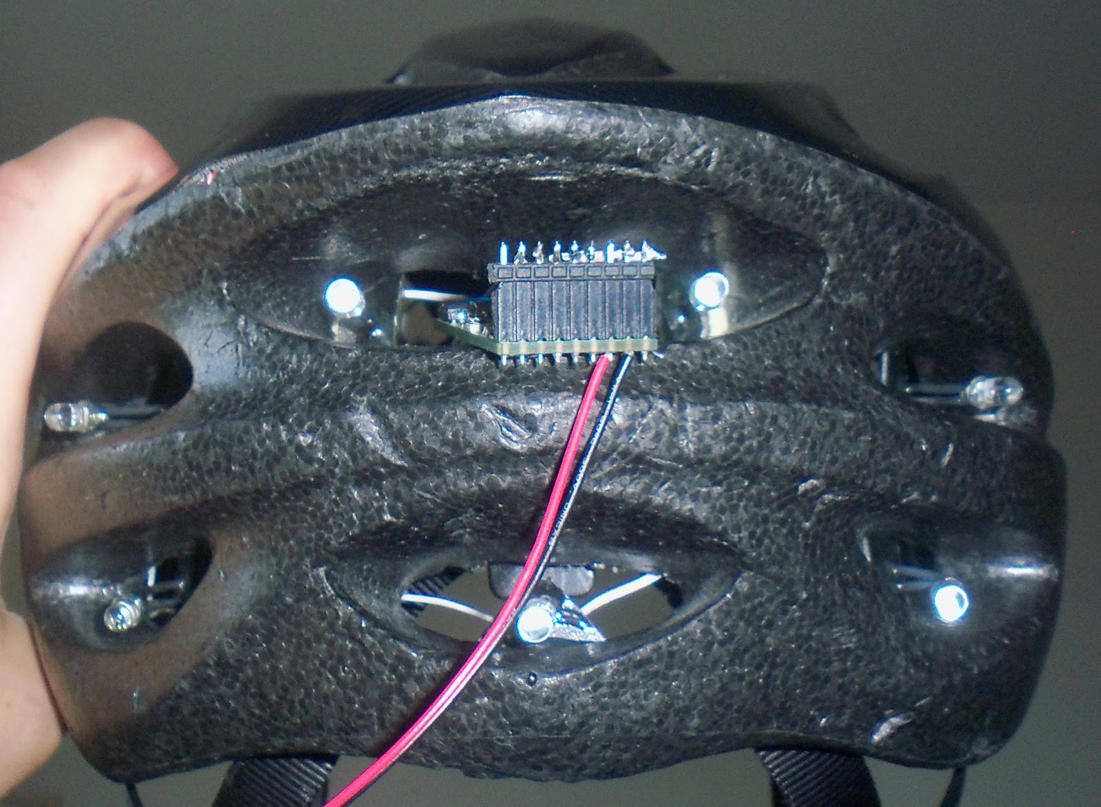
The outside of the helmet is shown below; first from ahead, then from behind.  The LEDs are mounted within the hollows of the helmet, using folded-over staples as an initial anchor, then doused with two-part epoxy.


The helmet in action is shown below:

The helmet is shown from the inside below; the LEDs are wired in series.  The leads of the LEDs go through tough plastic strips which are anchored to the helmet with bent-up office staples; everything is further stabilized with a healthy helping of two-part epoxy.


The interface consists of three buttons adhered to the side of the helmet (visible in the video above).  Everything on the helmet should be water-proof (though the controller module and battery pack are not currently water-proofed, as they are very much prototypes).

Moving forward, I would want to optimize/shrink the controller module, and incorporate a lithium-polymer battery pack with USB charging; hopefully, this would allow the whole battery/controller module to fit within the hollows of the helmet (rather than having a tethered AA battery pack hanging off of the back, as it is currently)

Saturday, June 23, 2012

Sleep mask prototype assembly and initial testing (or, now that the hardware's built, it's only 90% of the project left to do)

The next step in the development of the Sleep Mask was fabricating the 'final' prototype, and doing some initial testing to make certain that there were no shorts.

The front and back of the assembled board (with battery and display attached) are shown below.  The smallest surface-mount parts (including the charger and headphone amplifier ICs) were placed on syringe-applied solder paste and 'baked' into place using a cheap electric skillet; the remainder of the parts were applied manually, using a conventional iron (the reason for this roundabout assembly method is detailed in a previous post; long story short, I bought the wrong paste).

Being extra-cautious, I checked each of the solder joints on the tight-pitch ICs before adding the rest of the components.  Being extra-paranoid, I introduced cuts into the power traces, so that I could monitor current usage as I re-connected different subsystems (this is evident in the backside image).

Front of assembled board; display not yet mechanically fixed
Back of assembled board; display not fixed; connector to mask lights/sensor at bottom

With everything reconnected and no programming loaded into the controller, the device drew 4.6mA; with phones plugged in (and, again, no programming and thus no signal being output), the device drew 44.5mA.  Even with the tiny battery I have connected now (450mAh), this is low enough to allow for a full night's use on a charge; of course, this doesn't take into account the power used by the IR REM sensor illuminator, the display or the extra power which may be expended to generate actual sounds with the headphones.  However, power use appears to be dominated by the audio system, so I am not too concerned right now.

I connected the assembled board to the mask (shown twice below); additionally, the display is scotch-taped to the board to secure it mechanically (but reversibly so).


The only things left for the hardware are to fix the board and battery to the mask and to install the red LEDs in the eyecups (these will be used to flash at the user during alarm conditions).  I'll also need to install a header to allow for repeated programming.  All that's left for the software... is everything.

Or course, this is the roughest sort of prototype, meant to prove the concept and develop the basic REM detection algorithms and the framework of the eventual overall program architecture.  In addition to about a million changes to the overall mechanics of the mask (formed neoprene base? injection-molded face for the buttons/display), the main board itself would undergo a lot of beneficial changes, mostly to decrease its size.  As I've commented before, the components I've used are ones I have a stock of locally; as such, they are rated for far more current/voltage/power/dissipation than needed for the current application.  Additionally, the controller is the easy-to-hand-solder TQFP, rather than the absolute smallest package available.  As a result, I suspect that a future version of the device, with all the same functionality but reduced part size, could be as small as one quarter of the area of this version.


Sunday, June 10, 2012

Project updates (or, trading a few milligrams of epidermis for a few milligrams of reflowed solder)

Due to travel (and actual, legitimate research), I've not been able to progress on these projects much in the last few weeks.  Additionally, getting the boards from Seeed took a little while (though it was worth it, 10 boards for 15$ is nothing to sneeze at; they're shown immediately below).


Today, I got back into things by trying out a little hot skillet reflow.  Going off of resources at SparkFun and this instructable, it seemed the cheapest method available to me.  To apply the paste, I didn't have the time, money or patience to do solder paste stencilling (shown in the previous links); so, I applied the paste manually, as at this site.  Unfortunately, I didn't realize that the paste formulations are different between stencil and syringe application; I loaded some stencil paste from Sparkfun (here) into a syringe and it was very tough to get it to come out.

One thing to be aware of with the stencil-type solder paste: it behaves a lot more like wet sand than any sort of easily-coaxed gel.  Syringe-type paste might behave a little better/differently.

In any event, I was able to reflow the majority of the components on the (hastily thrown together) helmet flasher board, shown below (apologies for the poor picture quality).  I have seen heating-element control boards for toaster ovens and skillets to get the perfect heat profile; in my case, cranking the thing up to max temp and waiting for the solder to turn shiny sufficed.  Note the blue wire fix; I forgot to connect the enable line for the step-up to a free pin on the controller.


Debugging revealed only two small errors in the reflow; two of the pins on the stepup controller were bridged (easily separated) and one of the resistors in the current controller didn't reflow (also easily rectified).  The step-up produces 'high voltage' (16.5V), the pots have all been manually set (one to set the high voltage level, the other two to set the maximum constant-current levels) and the controller talks to my programmer.

The next steps for this quick project are A) create a simple program for this thing, and B) assemble the in-helmet parts of the project (lights, switches and 2xAA battery pack installed, wiring routed).  There's also the more pie-in-the-sky goal of implementing the EL drivers (but I haven't quite sourced the transformers yet; not enough of my CFL bulbs have gone out yet).

Of course, just because the project has barely started doesn't mean I'm not already thinking about version 2; specifically, I'd want to implement the following changes:
A: source smaller components, with specs sized more appropriately for this project.
B: add a LiPolymer battery and charger circuit to allow the controller module to be more monolithic and allow it to be charged over micro USB.
C: figure out a better connector solution between the helmet and the controller; the 0.1" headers I'm using were chosen for inventory convenience.