Showing posts with label REM Sleep Mask. Show all posts

Thursday, October 25, 2012

REM detector + display updates (or, scrolling displays are almost as cool as fezzes)

As I remarked in a recent post, I've nailed down the cause of my pesky REM detector noise issue.  Additionally, I started sprucing up the display subsystem, using a DMA channel to significantly reduce the processor load needed.  I've taken another couple of steps forward, in that I've implemented a fix to the REM noise issue, and I've refined the display subsystem so that it can easily produce text and primitive graphics; these refinements are shown immediately below.

The bottom 3/4 of the display is the REM differential signal level, scrolling from left to right.  The numbers on top are the 32-bit integer holding the device's seconds counter (left) and the IR illuimnator level (right).

Not very interested waveform-wise, but a clearer picture.


The video shows the scrolling display in action; since the sensor is pointed at the couch arm, there's not much going on, except when I rotate it.

Implementation details, vaguely

On the display side, this is really only a slight complication of what I outlined previously; there's a local buffer that I draw on, and periodically I set the DMA channel to transmit the contents of that buffer to the display via the serial transmitter peripheral.  There's a little bit of trickery translating the signed ADC inputs into the bytes that get painted into the display buffer, but it's overall quite straightforward.  A zipped archive of the project files is here.

On the REM detector side, I'd determined that the reason I was getting 'bias noise' every four samples was that the PWM switching transients were making it into the ADC signal, and because the PWM and REM counters were not integer multiples of each other, they would only 'line up' every four samples.  To rectify this scenario, I modified the code to make sure that the sample timer is always set up to be an integer multiple of the PWM timer period.  I also set up the clocking of the timers to go through the XMEGA's event system, so that I could keep the timers in sync.  A plot of the signal below shows no abnormal patterns in the noise, so I think this has taken care of the problem.


Moving Forward again

So, my next step has to be nailing down the REM detector.  Specifically, I'm going to slightly modify the hardware so that I can quarter the PWM duty cycle.  This way, I can maximize the settling time between the PWM switching time and the ADC sample time.  After this is done, I'm going to assess whether this has had the effect of decreasing the noise; either way, I'm going to collect some real-life sleep data, and get cracking on whether I can assemble a filter/classifier that can detect REM.

Of course, this completely avoids the issue of the busted charger circuit; unfortunately, I still haven't secured access to a hot-air rework station...

Wednesday, October 24, 2012

Using DMA to automatically transfer display data (or, it's RTFM, not 'Haphazardly Cast Your Eyes Left to Right Over The Manual While Thinking of Something Else')

As an aside from the process of perfecting the REM detector, I decided to start to clean up the display-painting parts of the firmware.

It takes half a kilobyte of data to completely fill the display (128-by-32 off-or-on pixels) and the data is sent through one of the chip's serial peripherals.  Since there is so much data to transmit per display update, it takes a LOT of processor cycles to do so; it takes even more cycles to do so by waiting and polling the serial peripheral instead of setting up an interrupt (as I did to debug the display).

Since the process of getting that data out to the display could be fairly straightforward, it seemed like the perfect excuse to take advantage of the AVR XMEGA microcontroller's onboard DMA feature.  And since I made a couple of errors along the way (and couldn't find a straightforward explanation of my problem online), it seemed appropriate to describe the situation here.

What is DMA?

Briefly, DMA (direct memory access) is a way of taking the load off of the processor by 'automating' data transfers.  Specifically, the DMA controller transfers a block of data from one location in memory to another while the processor executes other tasks.  Without a DMA controller, any large data transfer would take up processor time as the processor accessed and copied each byte of data individually.

There are many situations where you would want to transfer a lot of data from one location to another, or a small amount of data from (or to) one location a great many times.  In my scenario, I have a buffer in local memory that represents what the display will look like; the buffer is local so that manipulating it (compositing the image, blanking regions, adding text) is easier.  However, that buffer data needs to be periodically sent (serially) to the display hardware.  Ideally, the DMA will automate the process of taking each byte of the buffer in turn and sending it to the serial peripheral when it's ready to accept the bytes.

Implementation on the XMEGA

The XMEGA A microcontroller that I'm using has four independent DMA channels.  Each of them has a lot of configuration, including the ability to specify the source and destination data addresses and the ability to set what triggers the data transfers.

My problem was that I didn't read the manual closely enough; I thought that setting the channel trigger to the serial peripheral meant that every time the send register was empty (the trigger source), that a single byte would be sent.  In the default mode, however, the trigger causes the DMA to transfer an entire block of data as quickly as possible; since the serial peripheral sends out bytes a LOT slower than the rate that the DMA controller pushes bytes, this meant that each transfer only resulted in a few randomly-selected bytes of the buffer actually being sent to the display.  This caused me some consternation until I re-read the manual and realized my error; this fast operation is useful when copying data into SRAM or other fast destinations, but completely inappropriate for slow, single-byte destinations like the USART peripheral.

For slower destinations which will need to signal the transmission of each byte (or each burst of 2, 4, or 8 bytes) one at a time, the 'Single-Shot Data transfer' mode is used.  This mode completes a single burst, instead of a whole block, with each DMA channel trigger activation.

Since I want to transfer the complete contents of the display buffer to a single address on the serial peripheral, I need the destination address to be fixed and the source address to increment during the transmission, and reset at the end for the next update.

The actual C code I used to initialize the DMA controller and channel on the ATXMEGA128A4U is shown below; USARTC1 is the serial peripheral I'm using as my transmitter (it's been set up in master SPI mode for my display module, and then used to initialize the display module) and debugBuffer is the 512-byte-long stretch of internal memory that I'm using as my display buffer.

//set up a DMA channel
//enable the DMA controller
DMA_CTRL = DMA_ENABLE_bm;
//set the burst length to 1 byte
DMA_CH0_CTRLA = ( DMA_CH_SINGLE_bm | DMA_CH_BURSTLEN_1BYTE_gc );
//set the following: source address incremented, reload after each block; destination address fixed (reload after each block)
DMA_CH0_ADDRCTRL = ( DMA_CH_SRCRELOAD_TRANSACTION_gc | DMA_CH_SRCDIR_INC_gc | DMA_CH_DESTRELOAD_TRANSACTION_gc | DMA_CH_DESTDIR_FIXED_gc );
//now set the DMA trigger source to the USART data register being empty
DMA_CH0_TRIGSRC = DMA_CH_TRIGSRC_USARTC1_DRE_gc;
//load the block transfer count register with the number of bytes in our blocks (that is, 128*4 = 512)
DMA_CH0_TRFCNT = 512;
//now put in the initial source address; should be the memory address of the first byte of the display buffer
DMA_CH0_SRCADDR0 = ( (uint16_t) debugBuffer >> 0 ) & 0xFF;
DMA_CH0_SRCADDR1 = ( (uint16_t) debugBuffer >> 8 ) & 0xFF;
DMA_CH0_SRCADDR2 = 0x00;
//now specify the destination address; the transmit register of the USARTC1
DMA_CH0_DESTADDR0 = (( (uint16_t) &USARTC1_DATA ) >> 0) & 0xFF;
DMA_CH0_DESTADDR1 = (( (uint16_t) &USARTC1_DATA ) >> 8) & 0xFF;
DMA_CH0_DESTADDR2 = 0x00;

Once the DMA channel is set up (and assuming the USART and display have been initialized), I can update the display with the current contents of the buffer by simply enabling the DMA channel:

DMA_CH0_CTRLA |= 0b10000000;

Thursday, October 11, 2012

Project Updates (or, I am probably not dead)

So, it recently came to my attention that I haven't posted in several months.  This is due, in large part, to my actually getting work done on my PhD.  This is also due to the fact that the next steps are relatively... un-glamorous and un-postable.  Specifically, I have a small issue with the REM detector, and I need to figure out what's wrong with the battery charger circuit.  On the up side, I was able to significantly reduce the standby power consumption of my helmet flasher so... little victories.

Charger Debugging

As it stands, the Lithium-Polymer battery charging circuit does not work.  This is ironic, as it was the only sub-circuit that I did not mock up and test before ordering the circuit boards (I even mocked up the 3.3V buck converter, which only had three components).  I did this because, well... I was just using the reference implementation.  I've gone over the design (and the physical artifact's correspondence to it) with a fine-toothed comb; at this point, I'd like to swap the chip to see if that's the issue.  Unfortunately, I do not own a hot-air rework station, so that is easier said than done.  Additionally, the chip gets REALLY hot and sources a bunch of current when you plug it in, which complicates debugging, as I can only leave it plugged in for short periods.  Further, even if I could simply replace the chip, I'd be leery of doing it, as the new chip could easily fry as well.  This is triply annoying, as I would like to add the charger to my helmet and run signal glove in their next iteration, but can't do that until I know I've got the circuit right.

REM Detector Hiccups

The specific problem with the detector is that, for certain levels of illumination, the the detector output follows a 'negative bias' for every fourth sample; this is illustrated below.  Looking at the 'noise' and mean of the signal after separating it into four down-sampled signals (that is, the first sub-signal is every four samples of the original, starting with the first sample of the whole record; the second is every four starting with the second, etc.), it appears that this really is just a constant 'bias' term added only to every fourth sample.
This is an example of the detector output against my hand; green is the differential signal, dark blue is the single-ended signal, and light blue/cyan is the illuminator amplitude.  As you can see, the signal appears to get much more 'noisy' as the illumination level increases, until it abruptly decreases at a certain level.
Zoomed in view of the 'noisy' segment from above; we see that the extra 'noise' is due to every fourth sample being much lower than the other three.  This pattern is also borne out in the single-ended signal.
My current hypothesis is that this is due to my use of low-passed PWM outputs to give myself some extra low-bandwidth analog outputs to control the REM detector illumination level and the differential signal bias level.  Specifically, since the sample-specific noise only occurs at certain levels of illumination, and then suddenly stops once the level raises above that level, I am lead to believe that it's something to do with the PWM switching time lining up with the ADC sampling time.

If that's the case, I'll have to decrease the passing of switching transients by reducing the corner frequency of the low-pass and/or increasing the carrier frequency of the PWM.  Of course, increasing the carrier frequency will reduce the resolution of the LP-PWM channels; however, since I don't use the full resolution anyway, it wouldn't be much of a sacrifice.

Helmet flash controller standby power reduction

Going back to the helmet flasher project, I noticed that the AA batteries were getting drained in a manner that was less-than-consistent with usage.  I recalled that I had been less than diligent in regards to standby power usage, so I figured I could shave off a few milliamps by taking a closer look.

There were two main methods I figured I could use to reduce standby power use: put the controller into a deeper sleep state while in standby, and modify the hardware so that I could remove power from the op-amps used int he constant-current LED drivers.

The first approach, going into a deeper sleep state, was the first I implemented since it didn't involve modifying the hardware.  Before making my changes, I inserted a 1-Ohm 1% precision resistor to measure the standby current draw.  I set the device to go into "power down" when going into the standby state, with wake-up accomplished by state change on any of the buttons.  Additionally, I set the device to go into "standby" while the timers count and wait to move on to the next flasher state.  The source is available here, in case it is useful to someone wanting to see how a non-human primate would implement the preceding.

After implementing the sleep state changes, the standby power consumption went from 2.1mA to 1.7mA.  Good, but we're not finished.  Since the on-state power consumption is in the range of 100-200mA, it was impossible to detect if my changes had an effect on on-state power consumption.

The next step was to switch off the power to the linear constant-current LED driver block.  The op-amps used in that block draw current even when the LEDs are off, so it made sense to try to switch the power off when the device was in standby.  Since the analog block was currently fed directly from the power rail, it was necessary to cut that source first.

Since the op-amps only draw a few milliamps (far less than the 30mA the controller pins are rated for), it made sense to feed them from one of the controllers output pins; this way, I didn't need to add any additional FETs.  After doing this, and making the appropriate changes in the firmware, the standby power consumption fell from 1.7mA to less than 0.1mA.

Overall, these changes reduced standby power consumption from 2.1 to 0.1mA; a more than 95% reduction.  This makes me much more comfortable with leaving the batteries in when I'm not using it.

Next Steps

So, the most immediate next steps involve fixing the REM detector problem outlined above and making the charger circuit work.  After that, though, there are a couple of immediate next steps:

Finally finalize the sleep mask hardware

The current version of the sleep mask hardware is... clunky.  Pointy.  Eye-pokey, even.  Since it was a first prototype, I didn't put all the effort in the world into optimizing the layout, or the parts (I just used the components I had on hand, instead of sourcing the absolute smallest I could find).  Once I'm confident that the hardware is up to snuff, I can source the absolute smallest components (especially the controller and FETs/op-amps and the passives) and re-design the board.  To do that, though, I need to rectify the problems listed above (REM four-sample noise, charger broken).  Additionally, I'll need to take a few nights' worth of data and specify a classifier/filter that can detect 'REM' to my satisfaction; if the hardware needs revision to get to that point, I'd rather do so before the next hardware revision.

On a somewhat unrelated point, I'm going to hack up the headphone amplifier hardware to see if I can't make it more efficient.  As it stands, the white noise component consumes the lion's share of the power for the device.  Looking at the output of the headphone amp, the 'square edges' of the DAC output are preserved to the output; this might be causing greater power consumption than necessary.  If I introduce a high-pass before the headphone amp and shave those square edges off, I might be able to significantly reduce my power consumption.

Update the helmet flasher and glove turn signal hardware; make a decision about the helmet

As I've said above, I'd like to make the turn signal glove and helmet flasher run on rechargeable lithium-polymer batteries.  To do that, I need to make sure that the charger chip and circuit work as advertised.

Additionally, I need to make some decisions about the helmet flasher.  As it stands, it steps the battery voltage up to 16V to drive the LEDs in series.  This was done partially since I originally had intended to add some EL wire to the helmet; EL wire requires ~150V AC, and my intent was to switch current through some step-up transformers.  The transformers could be smaller/have a lower turns ratio if my switched DC voltage was larger.

This step-up is expensive (3$ for the controller alone, to say nothing of the related caps and inductor).  However, the series wiring of the LEDs allows the brightness/current of the LEDs to be more consistent.  Maintaining the step-up would also mean that I wouldn't have to re-wire my existing helmet.

Design the sleep mask PCB version 2

As I said above, once the sleep mask hardware is finalized, I'll source smaller components, and then redesign to the circuit board.  I figure it will be installed above the nose in the mask, with leads going down to the REM detector and red LEDs.  I'll also incorporate power control of the analog block, as I did for the helmet above, to reduce standby power consumption.

Order new boards + components; assemble + test

Just what it says: pick the new smaller components, order them and the boards, then build everything.

Software development of the sleep mask

At this point, the hardware for the sleep mask should be more-or-less finalized.  All that will be left is putting together the firmware.

I haven't given a lot of thought to the design of the interface or the overall design of the firmware.  However, I have given some thought to potential features I can try out, including:
  • REM-relative wake-up alarm: only wakes you up if you are at the tail end of an REM cycle (or you've reached some no-later-then-this time).  I haven't checked the science behind this, but I've heard that you wake up more refreshed if you wake up at the end of a cycle, rather than during the deep sleep in the middle.
  • Sleep induction using entrainment: again, I haven't looked into how rigorous the science is behind this is, but some advocate the use of binaural beats or isochronous pulses to induce lower-frequency EEG states, assisting the user away from consciousness.
  • External cues for lucid dreaming induction: the original purpose.
  • Slowly increasing LED illumination to ease wake-up: just what I said, improve wake-up by gradually increasing illumination within the mask along with the natural dawn.
  • REM logging: save the timestamps of REM periods, allow them to be transferred over USB.  Share on facebook?
  • USB bootloader: I know that Atmel provides one, I just need to see where it's hosted and play with it.


Saturday, June 23, 2012

Sleep mask prototype assembly and initial testing (or, now that the hardware's built, it's only 90% of the project left to do)

The next step in the development of the Sleep Mask was fabricating the 'final' prototype, and doing some initial testing to make certain that there were no shorts.

The front and back of the assembled board (with battery and display attached) are shown below.  The smallest surface-mount parts (including the charger and headphone amplifier ICs) were placed on syringe-applied solder paste and 'baked' into place using a cheap electric skillet; the remainder of the parts were applied manually, using a conventional iron (the reason for this roundabout assembly method is detailed in a previous post; long story short, I bought the wrong paste).

Being extra-cautious, I checked each of the solder joints on the tight-pitch ICs before adding the rest of the components.  Being extra-paranoid, I introduced cuts into the power traces, so that I could monitor current usage as I re-connected different subsystems (this is evident in the backside image).

Front of assembled board; display not yet mechanically fixed
Back of assembled board; display not fixed; connector to mask lights/sensor at bottom

With everything reconnected and no programming loaded into the controller, the device drew 4.6mA; with phones plugged in (and, again, no programming and thus no signal being output), the device drew 44.5mA.  Even with the tiny battery I have connected now (450mAh), this is low enough to allow for a full night's use on a charge; of course, this doesn't take into account the power used by the IR REM sensor illuminator, the display or the extra power which may be expended to generate actual sounds with the headphones.  However, power use appears to be dominated by the audio system, so I am not too concerned right now.

I connected the assembled board to the mask (shown twice below); additionally, the display is scotch-taped to the board to secure it mechanically (but reversibly so).


The only things left for the hardware are to fix the board and battery to the mask and to install the red LEDs in the eyecups (these will be used to flash at the user during alarm conditions).  I'll also need to install a header to allow for repeated programming.  All that's left for the software... is everything.

Or course, this is the roughest sort of prototype, meant to prove the concept and develop the basic REM detection algorithms and the framework of the eventual overall program architecture.  In addition to about a million changes to the overall mechanics of the mask (formed neoprene base? injection-molded face for the buttons/display), the main board itself would undergo a lot of beneficial changes, mostly to decrease its size.  As I've commented before, the components I've used are ones I have a stock of locally; as such, they are rated for far more current/voltage/power/dissipation than needed for the current application.  Additionally, the controller is the easy-to-hand-solder TQFP, rather than the absolute smallest package available.  As a result, I suspect that a future version of the device, with all the same functionality but reduced part size, could be as small as one quarter of the area of this version.


Sunday, June 10, 2012

Project updates (or, trading a few milligrams of epidermis for a few milligrams of reflowed solder)

Due to travel (and actual, legitimate research), I've not been able to progress on these projects much in the last few weeks.  Additionally, getting the boards from Seeed took a little while (though it was worth it, 10 boards for 15$ is nothing to sneeze at; they're shown immediately below).


Today, I got back into things by trying out a little hot skillet reflow.  Going off of resources at SparkFun and this instructable, it seemed the cheapest method available to me.  To apply the paste, I didn't have the time, money or patience to do solder paste stencilling (shown in the previous links); so, I applied the paste manually, as at this site.  Unfortunately, I didn't realize that the paste formulations are different between stencil and syringe application; I loaded some stencil paste from Sparkfun (here) into a syringe and it was very tough to get it to come out.

One thing to be aware of with the stencil-type solder paste: it behaves a lot more like wet sand than any sort of easily-coaxed gel.  Syringe-type paste might behave a little better/differently.

In any event, I was able to reflow the majority of the components on the (hastily thrown together) helmet flasher board, shown below (apologies for the poor picture quality).  I have seen heating-element control boards for toaster ovens and skillets to get the perfect heat profile; in my case, cranking the thing up to max temp and waiting for the solder to turn shiny sufficed.  Note the blue wire fix; I forgot to connect the enable line for the step-up to a free pin on the controller.


Debugging revealed only two small errors in the reflow; two of the pins on the stepup controller were bridged (easily separated) and one of the resistors in the current controller didn't reflow (also easily rectified).  The step-up produces 'high voltage' (16.5V), the pots have all been manually set (one to set the high voltage level, the other two to set the maximum constant-current levels) and the controller talks to my programmer.

The next steps for this quick project are A) create a simple program for this thing, and B) assemble the in-helmet parts of the project (lights, switches and 2xAA battery pack installed, wiring routed).  There's also the more pie-in-the-sky goal of implementing the EL drivers (but I haven't quite sourced the transformers yet; not enough of my CFL bulbs have gone out yet).

Of course, just because the project has barely started doesn't mean I'm not already thinking about version 2; specifically, I'd want to implement the following changes:
A: source smaller components, with specs sized more appropriately for this project.
B: add a LiPolymer battery and charger circuit to allow the controller module to be more monolithic and allow it to be charged over micro USB.
C: figure out a better connector solution between the helmet and the controller; the 0.1" headers I'm using were chosen for inventory convenience.

Sunday, May 6, 2012

Project updates (or, why is it that the least interesting parts of a project make up most of the effort?)

In the last few weeks (since I tested out the OLED display), I've been getting all of the last little details in place to move forward with the sleep mask project.  Specifically, since the circuits have been finalized, I have been laying out the printed circuit board and making certain that I have all of the necessary components on hand (and putting together an order for those I do not).

The cheapest service I could find is Seeed Studio's Fusion PCB service.  For a mere 10$ you get 10 5x5cm boards; an extra 15$ gets you 5x10cm.

After completing the board layout (shown below), I found that it was more than 5x5cm.  It is larger than I had hoped, but still reasonable relative to the size of the sleep mask.  A large part of its... largeness... is due to the fact that I was designing based on the parts I already had in my inventory.  Those parts, in turn, were chosen to be usable across many projects; as a result, they are usually rated for much higher voltages, currents, and dissipated energies than are strictly necessary for this project.  This is okay for a prototype, but any future hardware revisions will involve specifying more appropriately-sized resistors and capacitors.

Since I was going to have to pay for an extra 5cm of board, I decided to make the best of it and add a circuit for a project I've had on the back burner for a while.  Specifically, I want to build some flashing lights into my bicycle helmet for safety; some of the lights will be ordinary LEDs, but eventually I want to build some EL wire into the helmet to give a real Vegas feel.  To do this, I need 'high voltage' (about 20V) to step up to 120V using transformers.  While I am still collecting the transformers (I take them out of burned-out CFL lightbulbs, as transformers or even bare magnetics of appropriate size have proven difficult to source), I am going to move forward with getting this board, including the 20V step-up and LED constant-current drivers, layed out and ordered.  It is also shown in the image below.


The REM sleep mask board is on the left; the microcontroller is in the middle, with the micro USB connector above, battery charger above right, buck converter right, REM detector bottom left, headphone amplifier left and OLED display top left.  The helmet flasher/boost board is on the right; boost top left, EL wire switches bottom left, microcontroller bottom right and LED drivers top right.

Saturday, April 21, 2012

SPI OLED A-OK (or, I would like to apologize to my readers for the preceding title)

I've reached another milestone in the development of my sleep mask: the OLED module works.

This section of the project was relatively straightforward: basically nothing more complicated than establishing a serial connection to the device and starting it up appropriately.

The Hardware

This is identical to my original design, which was, in turn, copied from the module datasheet.  This is the same hardware as is sold by Adafruit Industries; I acquired mine from another source, without the breadboard-friendly PCB attached.  It has an on-board capacitor charge pump to provide the high-voltage (~7.5V) necessary to drive the OLED pixels.  The serial interface is identical to the Serial Peripheral Interface (SPI) with a Command/Data select line and a Reset line in addition to the usual Chip Select line.

The Software

The stripped-down testing firmware I used is posted here.  It's not much to look at; it just starts up the SPI on-chip peripheral and sends the necessary command bytes (while manipulating the control lines appropriately) to start up and activate the display module.  It then starts sending out data bytes to change what is shown on the display.  The commands sent are outlined in the module controller's data sheet (the Solomon Systech SSD1306).

The controller continuously updates the pixels in the display by reading from an internal display memory.  When data is written to the device, it is used to update the contents of this display memory.

The folks at Adafruit have also implemented some software to drive this display module.  My software is largely the same, with one noticeable difference.  The controller contains twice as much display memory as needed for the module (to make it capable of driving larger displays); when writing to this memory over the serial link, the memory is all written over in turn before restarting at the beginning.  The Adafruit software just writes zeros onto that second half of the driver memory; however, there is a command which allows you to set the limits of the memory to be written.  By setting this command to only write over the usable half of the memory, my software doesn't need to write the entire memory every time, only the half that is actually visible.  In this way, I don't need to devote as much of my computational resources to updating the display.

The Goods

The test hardware setup is shown below.  As usual, I used my oh-so-refined soldering and fabrication skills to gain access to the tiny pads on the end of the display's ribbon connector.  The connections are relatively simple; a few decoupling caps between power pins to ground, some pass-throughs for the serial link, and the two capacitors for the charge pump.


To prove that I actually got this to work, here is a short video of the device (and ATXMEGA controller) as power is applied; first the display is told to turn all the pixels on, then it displays from the display memory (which is, initially, full of noise; this is in contrast with the data sheet, which states that the RAM should be blanked after a reset cycle).  Then, the controller starts sending alternating frames of display data.


The firmware source containing the specification of the alphabet/symbols is here.

Sunday, April 15, 2012

REM detection hardware, firmware and software tests (or, I honestly had some doubts that this would work so well)

On the REM-detecting, white-noise-generating, potato-julienne-ing project front, I have finalized the hardware (and toyed with the firmware) for the REM detector subsystem.

To recap this project: I am developing a sleep mask which will be able to detect the REM (rapid eye movement) phase of sleep, and wake the user up at the 'optimal' point in their sleep cycle.  Additionally, it will be able to record the timing and duration of REM sleep phases (potentially useful for improving sleep) and it will be able to generate white, pink or red noise through speakers at the ears to improve sleep.

I mocked up the hardware and some firmware which sends acquired REM detector samples over a serial channel; I also had to put together some software to acquire, interpret and plot this serial information.  The results of this effort have allowed me to finalize the hardware design for the REM detector subsystem.  As it stands, all I have left to finalize of the hardware is the display and the USB interface hardware; once these two things are nailed down, I can design and order the boards and fabricate the hardware, moving to the firmware-only phase of the project.

Finalized hardware

The hardware has been modified from the schematics I presented originally.  These changes are due primarily to two factors: the microcontroller has an internal gain (negating the need for a second external gain stage) and the desire to used a switched-emitter topology (that is, the illumination of the eye for REM detection will only be on for a small percent of the time to save power).

As seen in the schematic below (the left op-amp), the current output from between the phototransistors on the mask is fed into a transimpedance amplifier whose output is fed directly into an ADC pin on the microcontroller.  This single-ended signal can eventually be used to set the emitter amplitude.  This signal is also fed into the positive side of a differential ADC (with gain); the negative side is fed from a lowpassed PWM output.  This negative input can be used to bias the differential ADC channel to maximize dynamic range; the lowpass converts the oscillating PWM signal into a DC signal whose level is the rail voltage times the Duty Cycle of the PWM waveform.  The transimpedance amplifier feedback resistor is set to 40kOhm to maximize signal amplitude while preventing saturation under normal (and even some abnormal) usage conditions.
The driver circuitry has been significantly improved in this schematic.  Specifically, an op-amp is used to 'linearize' the current control.  Above, a sense resistor is used in negative feedback to set the current through the infrared emitter; the set point is determined by a lowpassed PWM fed through a voltage divider.  Without the 'linearization' of the sense resistor and negative feedback, the highly nonlinear nature of the emitter's current/voltage characteristic meant that only a few of the possible PWM output levels were 'useful' (that is, corresponding to levels of current we would want to drive our emitter with).

Additionally, the op-amp makes driving the emitter simpler; its high input impedance simplifies the design process for the lowpass-PWM easier.  Additionally, it makes it simple to add an enhancement N-FET to allow for switching the emitter on and off (by tying the control input of the op-amp to ground).

Firmware/Software for debugging

To debug the REM detector hardware, I needed to implement a firmware to sample the REM detector input channel and transmit that data to my laptop.  I also needed to create software on my computer to acquire and plot the transmitted serial data.  The firmware and software are contained in this zip archive.

The big questions I needed to answer were: what do I need to do to keep the differential channel biased appropriately, and how long does the emitter need to be on to ensure that the phototransistor signal is stable before sampling.

The firmware samples the single-ended and differential ADC channels.  It then updates the PWM bias setting on the negative input of the differential channel to keep the differential signal centered.  It then formats a couple of serial bytes according to the ADC data and sends them to the computer.

To plot this serial stream, I made a function in MATLAB that opens the serial port and continuously samples the incoming bytes, breaking up the stream into sequences, translating them into floating-point numbers and displaying them on the screen, as seen below.  The blue trace is the single-ended ADC channel, the green trace is the differential channel, and the red is a moving-average of the green.

I waggled my eyes at the beginning and middle of the plotted waveform; you can see that the signal is well-modulated by eye-waggling, which is necessary for detection of REM.
I used a USB oscilloscope (the Hantek DSO-2090, highly recommended) to check out the settling time for the phototransistor signal in response to switching the emitter.  At the end of the day, I established that a switched emitter could be timed to allow for detection of REM using the specified circuit, so I have finalized that circuit and am moving on to validating the USB and display subsystems.

Sunday, March 11, 2012

Generating and outputting white, pink and red noise (or, all that effort just to generate signals you'd usually rather be without)

I've completed the design and verification of the noise generation software and hardware.  I have finalized the software for generating colored noise from white noise samples and I have mocked up the headphone amplifier circuit and verified that it works and performs as expected

CPU use by noise generation algorithms

One important last step in implementing the colored noise generators is determining how long they take to execute.  If it takes 300 cycles to generate a single sample of pink noise, and you've only got 200 cycles to do it per sample, you're going to fall behind.  Alternatively, the algorithm could take on average 100 cycles to complete, but 210 cycles in the worst case; what do you do to handle that worst case?  Additionally, how many extra cycles do you need per sample to do housekeeping tasks and run other subroutines?

In my situation, I need to generate a noise sample at regular intervals.  If the generator, on average, costs more cycles than you've got, you can increase your clock frequency, decrease your sample rat or try desperately to increase the efficiency of your code.  If the average execution time is good, but the worst-case takes too long, you can perform the above interventions or write some sort of wrapper function that keeps a sample or two generated ahead of time, to allow for the worst-case samples.

Looking at the actual execution statistics, however, leads me to believe that I have a more than acceptable margin even in the worst cases.  To get real, live cycle costs, I coded up a firmware that looks at a counter immediately before and after use of the algorithms, then transmits the difference over the serial port.  I then left the thing to run for about a second's worth of data (about 44100 samples for each of the three generators); the summary stats are:

  • White Noise: 10 cycles average, 10 cycles worst case, 10 cycles best case
  • Pink Noise: 90 cycles average, 99 cycles worst case, 88 cycles best case
  • Red Noise: 56 cycles average, 70 cycles worst case, 52 cycles best case

Since I'm running the CPU at 32MHz, and my sample rate is 44100Hz, that give me about 725 cycles per sample to get thing done; several times more than a comfortable margin even in the worst cases.  Since I am likely to only be generating the samples in a mode where other interactions/tasks are minimized (that is, not much else should be going on while the user has the device on), it may even be possible to reduce the CPU speed to improve battery life.

Verification of amplifier hardware design

I'm using Maxim's MAX9724B fixed-gain headphone amplifier IC.  I chose this part because:

  • It's monolithic: feedback resistors are internal and issues with stability and such have been taken care of by Maxim's engineers.
  • It contains a charge-pump voltage inverter to allow for bipolar output simply and easily from a positive rail; this allows for louder maximum output and removes the need for large output DC-blocking capacitors.  Additionally, if I end up needing a negative rail for other things, the device is designed to provide a little more current than it needs.
  • Click-and-pop suppression, RF noise rejection, very small package size.

Here's the chip, connected to the necessary capacitors and headphone jack.  I soldered onto that extra-tiny 12-pin TQFN by hand (this was a ridiculous experience).


I plugged everything in, and it worked.  The voltage on the charge pump output was -3.3V, and the headphone outputs sounded good.  I hooked up the scope to the outputs to see if the amplifier was rounding out the DAC switching transitions.  They were slightly rounded, but still very obvious.  However, as I just said, the outputs sounded okay, so I don't feel the need to alter the design to include lowpassing to get rid of the last of the switching transitions.

Next Steps

The only bits of hardware left to verify are the display and the REM detector; of course, these are likely going to be more difficult than the preceding hardware and software.  The display should be fairly straightforward in hardware, but coding the drivers will be more involved; It may be possible that someone has already implemented such software and I can crib off of that.

From the little bit I've already done prototyping the REM detector, it's likely to be somewhat temperamental.     The level of illumination provided by the IR LED has to be large enough to result in a big REM signal, but small enough that the zero-frequency current offset saturates the transimpedance amplifier.  It seems likely that the optimal illumination level will change between users and possibly even for single users between uses. As a result, I'll likely need to code in a feedback controller to optimize the illumination level for whatever the current operating conditions are.  I also need to nail down the properties of the REM differential current signal, to determine how often I need to sample the signal and whether it will be possible to gate the illumination signal in time with the sampling to minimize power usage.

(There is still the matter of the battery charge circuit; however, I trust the part data sheets and the IC has about a million pins, so manual soldering is going to suck if I try to mock it up.)

Saturday, March 3, 2012

Colored noise generation using a hardware CRC (or, 'it sounds right' is basically as good as mathematical rigor, right?)

Toward the 'noise maker' aspect of the sleep mask I'm designing, I've done some work toward generating white and colored noise on the AVR XMEGA hardware.  My goal was to generate white, pink and red/brown noise so that any of the three could be chosen by a user to aid their sleep.  So far, I have generated white, pink and red noise in simulation (using a model of the XMEGA's CRC generator) and have translated these simulations successfully to the actual microcontroller for the white and red cases. UPDATE: pink case also successfully implemented.

Background

Many devices and applications exist which generate various sounds/noises to aid sleep and drown out the irregular sounds which can interrupt deep sleep.  Three commonly provided sounds are white, pink and red noise; white noise has the most high-frequency content, pink less and red the least.

Colored noise

White noise refers, generally, to noise whose samples are totally independent of each other; knowledge of one sample gives no information about any other sample, previous or subsequent.  As a result, a white noise signal's autocorrelation is unity at zero lag and zero elsewhere.  Additionally, a white noise signal has equal power at all frequencies.  Different types of noise are commonly referred to by their 'color': white is so-called because it contains all frequencies, analogous to the way that white light contains all colors.  Pink noise is similar to white noise, except that it has a decreasing amount of power as frequency increases; where white noise has a constant power level (P(f) = 1, let's say), pink noise has 1/f power (P(f) = 1/f).  Red noise takes it a step further, having even less power at high frequencies (P(f) = 1/f^2).

Pink and red noise can be generated from white noise.  Red noise can be generated by integrating white noise (this is where its other name, brown/brownian noise, comes from: the path of the signal in time is a Brownian walk).  Pink is more difficult to generate; where red noise can be generated using integration or a first-order lowpass, generating pink noise would require some sort of half-order filter.  From my researches, there are two commonly-implemented methods for generating pink noise computationally from white noise: using a specially-specified higher-order filter, and the Voss-McCartney method.  These methods are quite capably and completely explained and expounded upon here and here; since the special filter method involved a lot of multiplication and tweaking and maybe even floating point math, I chose the Voss-McCartney method. It is very clever, and only relies on addition, subtraction and keeping track of a very small buffer of past-generated white noise samples.  I will go over it further when I describe my implementation below (I assure you, though, the sites above are quite top-notch).

Random and no-so-random numbers

The difficulty in generating white noise is finding a signal source whose output at one point in time is totally independent of its output at a subsequent time.  Or course, this is impossible with any normal computer system; its state at one clock cycle is deterministically derived from its state at the previous cycle.  It is possible to access randomness in the form of analog signals in the environment around the computer; if we have a bit of radioisotope, its decay will serve as a great random process.  A reverse-biased diode can also be used, as can the randomness in the timing of user interactions (if we happen to have a user close at hand).  The problems with the above hardware random number generators (and hardware random number generators in general) are twofold: first, the extra hardware can be expensive; second, the rate of random bit generation can be very slow (especially true in the case of the user input).

Faced with these costs, it would be nice if we could, deterministically within the computer, generate numbers which are random-like.  While the computer's state completely predicts the next pseudorandom number, the string of numbers in question may appear random enough for a specific purpose.  Since our success criterion is 'does it sound good', even a poor pseudorandom number generator (PRNG) will be good enough.  There are a variety of algorithms extant; Linear Feedback Shift Registers (LFSR) are one such class of PRNG.  They work by shifting a register and exclusive-OR-ing some of its members every clock cycle.  The XORshift algorithm is a cheap and capable method invented by George Marsaglia.  I implemented and tested a version of it (for the 8-bit platform, developed by William Donnelly) before I realized that the Cyclic Redundancy Check hardware on the XMEGA, intended to check the integrity of the program flash memory and USB transmissions, was also an LFSR and might afford me four bytes of decent pseudorandom numbers every clock cycle.

Hardware and software implementation

The central question going into this was 'will the hardware CRC peripheral be able to produce samples of data that sound sufficiently white?'.  I had already implemented the 8-bit Xorshift algorithm provided by William Donnelly, and it performed well.  However, it took over 70 cycles to generate one sample, so the possibility of ONE cycle samples was too good not to investigate.

Setting up and using the CRC to generate pseudorandom numbers

The CRC peripheral on the USB-capable XMEGAs is fairly straightforward: a control byte, a status byte, a data input byte and four output bytes.  It can take as input the flash memories, the DMA channels or a 'manual' single-byte IO channel, so that user applications can more easily take advantage of the hardware.  I had some difficulty with getting the thing to take my IO data and getting it to perform the full 32-bit CRC (instead of getting stuck in the 16-bit mode), so here's my sequence for initializing it for my nefarious purposes:

//set up the CRC thingy to accept data from the IO bus, CRC-32
//also set the current state of the CRC generator to all 1's (if //it resets with all 0's, this will go nowhere)
CRC_CTRL |= CRC_RESET_RESET1_gc;
//set up the input to be the data byte
CRC_CTRL &= CRC_SOURCE_gm;
CRC_CTRL |= CRC_SOURCE_IO_gc;
//set to 32 bit width; first set busy byte to allow the change
CRC_STATUS |= CRC_BUSY_bm;
CRC_CTRL |= CRC_CRC32_bm;


Every time I want to get a new random number set in the outputs, I feed all zeros into the CRC (other bytes may be valid), and read out the changed checksum a mere single cycle later.

//change the checksum
CRC_DATAIN = 0b00000000;
//get the bytes
uint8_t crc_out3 = CRC_CHECKSUM3;
uint8_t crc_out2 = CRC_CHECKSUM2;
uint8_t crc_out1 = CRC_CHECKSUM1;
uint8_t crc_out0 = CRC_CHECKSUM0;

Bear in mind that this set-up only works for my situation of steady-state generation of pseudo-random checksums by passing more and more constant bytes into the CRC hardware.  If the CRC hardware is required for other tasks (like, for example, checking out USB packets), it will be necessary to save the current state and reset the generator (including, possibly, changing the data source and bit width) before using it.  Before going back to using the CRC as a PRNG, it is necessary to pause the generator, load it with the saved state, and set the input and bit width as above.

To verify that I understood how the CRC hardware worked and how to access it, I created a firmware which generates a new CRC checksum (by adding an all-zero byte to the input) and transmits it over the serial peripheral.  The source is available here (that component is actually commented out in a big block in the middle).

Simulating a sequence of random numbers; implemented coloration

Using the data output over the serial channel above, I tested a MATLAB function which implemented the activity of the CRC as detailed in the device datasheet (available in this zip file, 'benCRC32guess.m').  Once I was satisfied that my model of its working was correct (bear in mind, that file assumes that the input to the CRC is all zeros), I used it to generate a sequence of bytes as the hardware would.  I then did the simplest test of white-ness possible: auto- and cross-correlation.

The first plot is the autocorrelation for the first byte of the CRC checksum; It is high for only one sample and low elsewhere (not sure why the scaling was all wonky).
The second test was cross-correlation between the bytes; even getting only one random byte per cycle would be great, but if I could use all four (that is, if they were also independent of each other) would be super-great.  As shown below, the cross-correlations were all nada (same weird scaling as above).
Note that the above two plots are exemplars (top was for byte 1, bottom was betwen bytes 1 and 2); the autocorrelations of the other 3 bytes and cross-correlations between the other 5 pairs were similarly acceptable.  The final (and most important) test was the by-ear test; does it sound right?  As linked above (and here), the white noise from the simulation sounded right.

Now that I was confident that the CRC PRNG method was acceptable, I moved on to implementing the red and pink noise generators.  The brown was the simplest; simply integrate the input from the white sample generated above (taking care to prevent values outside a finite range).  This first pass was okay... but exhibited some nasty clipping-ish atrifacts, due to the fact that I just put a hard limit on the valid range (that is... once you hit the ceiling/floor, you hit hard, and saturate).  To soften this, I set up 'buffer' ranges within the valid range.  The middle range allowed for integration as normal; however, progressively farther out ranges scale down input samples which would move the integrand away from the middle of the range.  This was implemented in the MATLAB file 'brownMakerSoftedge.m' in the zip file linked above (and here).  While I have no idea what this does to the statistics of the signal, it makes it sound better, and thus is awesome.

Implementing the Voss-McCartney algorithm for pink noise generation was slightly more involved (but only slightly).  While the links above explain in more detail the ins and outs of the algorithm and its statistical properties, I will describe it briefly here.  Basically, the output of the generator is the sum of 8 white noise generators.  Each generator is sampled progressively more slowly; the first generator is updated every sample, the second every two samples, the third every four samples...  Since each generator exhibits more and more low-frequency power, the sum of the set ends up having a more-or-less 1/f power spectrum.  By scheduling the updates appropriately, only two new white noise bytes are required every sample.  My implementation is in the MATLAB ZIP file, as 'pinkBuffer.m'; the sample sound is here.  As above, it sounds right, so it is right.

Porting the colorizers to the hardware

The MATLAB business above was more-or-less directly ported to C for compilation and loading onto the ATXMEGA32A4U.  The source is in these three files (various bits of code will need to be commented/uncommented).  I set up the generators to continuously transmit samples over the serial channel; these samples were read into MATLAB using the 'getSerialCRCtest.m' file in the ZIP archive.  They were then converted to floating point values, zero-meaned and scaled so that they could be exported as WAV files.  The hardware-generated white noise is here, and the hardware-generated red noise is here.  They sound good, so I'm satisfied.  Currently, the hardware pink output does not sound good (and, upon visual analysis, also does not look good), so I am still working on that.  UPDATE: I changed the source slightly, so the pink works now (and sounds right).  Modified source is here.

Next steps

The first step is to figure out whats going wrong with the XMEGA implementation of the Voss-McCartney algorithm.  Probably some sort of overflow issue.

The next step is to read up on the XMEGA DACs and start passing the generator outputs to the outside world.  After achieving that, I'll mock up the headphone amplifier and see if lowpassing is necessary to eliminate DAC switching transients in the output (if not, I can use the internal-resistor amplifiers, which would reduce overall parts count).

Once all of that is settled, I'll tidy up the code to make it more modular/portable, probably including a save/load state feature to allow CRC hardware use by other functions to be interleaved with the use here.

UPDATE: The pink noise generator works now.  Instead of updating the buffer sum, I completely re-calculate it with each iteration.  The modified source is here.

Sunday, February 19, 2012

REM-detecting white-noise-generating sleep mask (or, biting off more than you can chew)

For my next project, I'm going to design and build a sleep mask that has the ability to detect rapid eye movement (REM, which indicates dreaming sleep) and present sounds and lights to the wearer to enhance the sleeping experience.

First, the device will sound an alarm when the user is at the 'optimal' time to wake up, relative to their sleep cycle.  It's asserted in various places on the internet that the ideal time to wake up is at the end of an REM cycle; I'm still searching for peer-reviewed research to this effect, but there already exist devices on the market that trade on this possibly-more-substantial-than-folk wisdom.  Specifically, there is a headband that records EEG (brainwaves) to detect REM sleep, and a wristwatch which detects REM through arm/body movement and/or elevated heart rate (I can't tell how exactly it detects REM from the wrist, but those are my guesses).  Additionally, there are several smartphone applications and this alarm clock that detect REM through the amount of body movement a person exhibits.  I will detect REM directly, by illuminating the eye with pulsed infrared light and recording the changes in the reflected power.  The EEG headband device is very expensive, and my device will end up with a far wider range of features than both devices, so I don't think I'm duplicating any existing products.  Additionally, the timing and duration of REM cycles will be recorded and accessible by USB.

Second, the device will present noise to the wearer to assist in sleep.  I more-or-less need a 'red' noise generator running in the room to sleep well; devices on the market exist that produce white, pink and red noise as well as other 'nature' sounds to improve sleep.  By generating the noise in the mask, it becomes a sort of 'best sleep in a box'; with the alarm and noise generator, you can easily have as good a night's sleep in a hotel room as you do at home.  While there exist myriad smartphone programs to generate these noises (here is a site for a company that makes a good, no-nonsense one that also works for free on a computer), I don't own a smartphone.  So there.  Also, these features wrapped up into one common device elevates the mask to the status of a general sleep appliance that would be useful as a discrete device with one interface, one battery to charge and no monthly fee.

Third, the device will be able to deliver light and sound to the wearer during REM sleep to help induce 'lucid dreaming'.  Lucid dreaming is a state where you are dreaming, but consciously aware of that fact and thus able to influence the contents and progression of the dream.  The ability to dream lucidly is a talent that can be developed; one method is to train yourself to periodically perform 'reality checks' so that if you are dreaming, you will become aware of it as soon as your next 'reality check'.  There are also devices which attempt to present flashes of light or sound pulses during REM sleep which can indicate to the dreamer that they are asleep.  There already exists a 'commercial' product that attempts to do this called the NovaDreamer; it uses a simple delay to hopefully flash lights at the user during REM.  Since this device is no longer being made, and since it uses such a simple REM prediction method (that doesn't take into account any real-time information about the user), this feature is treading in a more-or-less untapped market.

Together, these features make a device that will, hopefully, allow the user to have more enjoyable wake-ups, better sleep and possibly troubleshoot their sleep by analyzing the recorded sleep cycle data.  Additionally, I will design the hardware with 'future-proofing' in mind: I will attempt to make features software-configurable and extensible so that A) features can be progressively added an debugged on the prototype hardware and B) extra features can be added beyond the immediate scope outlined above.

Overall system scope


  • The most important design constraint, considering our culture's current level of microelectronic and battery technology, is device size and shape.  I want this device to basically be a slightly bulky sleep mask; the battery and electronics/interface board will be mounted on the front of the eye-cups and small speakers for the noise generator will be built into the band (EDIT: this speaker-in-the-band approach has apparently been done before).
  • The device should be able to run for at least three nights without recharging, and should be able to be used while charging (I absolutely loathe cordless devices that can't charge while being used; burn in hell, cheap knock-off cordless drill!).
  • The interface should be quick and simple for common tasks but allow for more detailed settings to be accessed relatively easily; additionally, common during-sleep interactions like volume control and snooze should be easy to perform while wearing the device.
  • Charging, sleep data downloading and firmware updating should occur through micro USB port due to the ubiquity of micro-USB cables and chargers for cellphones (and even for dumb devices, of late).


Overall system design

Mechanical

The mechanical design will consolidate as much of the electronics as possible onto a single board over the left eye; REM detection will occur through emitter/detector pair whose leads go through the left eyecup; the battery will be mounted over the right eyecup; and the speakers will be built into the sleep mask's band.  Eventually it will make sense to design a hard plastic enclosure/casing for the electronics in and around the mask, but for now I'm going to focus on the electronic side of the design.

Electronic

The electronics will consist of several subsystems:
  • Power management: a Microchip LiPo battery charger IC will sit between the USB V+ rail, the LiPo battery and the application circuit.  Everything downstream of the battery will run off a +3.3V rail provided by a high-efficiency buck converter.
  • REM detection: the center of the detector will be an IR emitter and a pair of IR phototransistors.  the detectors will be stacked to allow for differential current measurement, which will be amplified by a transimpedance amplifier cascaded with an inverting gain stage.  All signals will be 'unsigned' (0 to +3.3V) and full dynamic range ensured by proper biasing.  This circuit is cribbed fairly liberally from an undergraduate project to implement REM detection for a sleep alarm (design document mirrored here).  A similar project  is  here.  Since the signal of interest is very low bandwidth, the emitter will be pulsed in time with ADC sampling of the output; this is a significant difference from the previous work and should result in significant power savings.
  • Noise generation: an attractively-featured Maxim headphone amplifier will be fed with the DAC outputs of the microcontroller.  The chosen amplifier breaks out the feedback path, allowing me to design in a suitable bandpass to cut off the high-frequency DAC switching transients and also block the +3.3/2V DC component in the DAC outputs.
  • Interface: the interface will consist of four appropriately labeled pushbuttons and a nifty ultra-tiny OLED display manufactured by Univision Technology Inc..  I was able to find two for cheap off eBay; I found the module and controller datasheets on the Adafruit website (here and here).  The module contains its own driver stepup and is controlled over SPI.
  • Controller: ATXMEGA32A4U.  I wanted built-in DACs and USB support; additionally, the timers for the ATXMEGA (along with most everything else) are very expansively featured and allow for 32MHz operation down to 2.7V.  Migrating to ATXMEGA from the ATTINY and ATMEGA I've played with in the past means that I needed to find a cheap PDI programmer; I found the ZeptoProg on eBay for reasonable cheap and it plays well with AVR Studio 6 (I tried to get it to play well with AVRDUDE and the open source toolchain I used to use... but the problems have not yet been resolved).

The minimum usable endurance for the device is one night; assuming a middle-of-the-line, appropriately sized LiPo battery of 1000mAH capacity, this means that our device needs to draw about 100mA in the mean.  Tallying up the current usage of the various subsystems in theory yields a number far less than this, but I want to plan for the worst in putting together the prototype.  The buck can handle more than 100mA, and the battery charger circuit was designed with trimpots to allow for an appropriately-sized battery to be chosen after the completed device has been tested for real-life current usage.

Software

I've only designed the software in the broadest strokes; there will be a 'mission' mode, wherein the device keeps time, generates noise and detects REM, and an 'interface' mode, where the user is navigating menus and setting things up.  The reason I plan to segregate this way is twofold: first, the user can't navigate most of the menus while wearing the device, so we'll never have to do both (generated noise/sense REM and generate the interface display); second, generating the random numbers for the noise might take up a significant fraction of the available processing power, so I want to leave as many cycles spare as I can during  'mission' operation.

For particular computational tasks, I have put together some research/notes and even performed some simulations to verify cycle costs and correct theoretical behavior.  Specifically, I've collected a number of online resources toward the task of generating reasonably white noise from pseudorandom noise generators on a microcontroller substrate (8-bit XORshift, wider XORshift, linear congruential generators).  Additionally, there are a couple of good online treatments of the problem of generating pink noise from white noise (here and here; while red noise is easy (just integrate), pink noise falls off as though passed through a 'half-order' filter, making the whole proposition interesting).  In a future post, I'll go over these methods and the results of my simulations/implementations.

Futureproofing

I cut off the ballooning feature list as outlined above; however, there is a lot left I want to implement.  Additionally, since this is a prototype, I wanted the design to be able to be implemented incrementally with the same printed circuit board; I am a poor, struggling, starving, barely-making-the-rent artist type so I really only want to order one version of the board.

For debug-proofing, the following features will be added, to allow for incremental feature roll-out

  • Test pads allowing easy access to the programming port and a simple UART.  This will allow for ease of programming before I figure out how to work Atmel's super nifty firmware-update-over-usb bootloader.  The UART will allow for debug information to pass easily from the device, and allow for proto-interfaces to be coded for the UART before I get the real SPI-OLED interface up.
  • Trimpots to set the charger IC's constant-current charge level and constant-voltage current threshold. Since the overall power usage is not 100% nailed down at this point, I wanted easy options for the battery.  Additionally, this allows me to eventually make the weight/cost/benefit tradeoff without having to pull up and replace set resistors on the board.
  • Pads and jumpers inline with the REM and noise signals paths.  This will allow me to troubleshoot problems with those subsystems (though I hope to have the circuits finalized through practical testing before I order the boards).
  • The option of a manual trimpot or microcontroller PWM control of the bias level for the REM circuit.  My current plan is to use the ongoing signal levels in the REM circuit to set the bias level, allowing for greater signal amplification without running into the edge of my dynamic range.  However, this may not be the best solution (or it may just take some finite time to implement), so I'm giving myself the option of manual setting via a trimpot.

As for future-proofing, there is really only one thing that I am altering the hardware for to possibly allow in the future, and that is a pulse oxygenation sensor.  This sort of a sensor would allow the device to have access to both the user's pulse rate (potentially improving the REM detection) and the user's blood oxygenation (a decent measure of the efficacy/rate of their breathing).  Being able to record these two things would make sleep-problem diagnosis with the device significantly more powerful.  Admittedly, my current knowledge of the practical tribulations involved in building a robust pulseox sensor is minimal; however, I know that I will need an analog input, two 180-degree out-of-phase PWM signals and two analog outputs to set the emitter gains (which I will implement with lowpassed PWM signals).

Additional futureproofing would involve adding a micro SDHC card slot to allow for datalogging of more user sleep data (especially if the pulseox is ever added).  Since, in terms of harware, this is as simple as connecting to an SPI port, I will add the footprint and pullup resistors at the end of the board design process if the added device size seems reasonable.

All of my other potential future features are software changes; for example, I might want to add some code to slowly bring up the visible LED levels to simulate sunrise, leading to better wake-ups.  By having the LEDs driven by PWM from the start, this should not require any hardware futureproofing.

Work to date

Beyond the general design work, I've begun to mock up sub-circuits to test them and refine the design.  Additionally, I've begun to modify a sleep mask with the various bits and bobs necessary to detect rapid eye movement.

I've mocked up the 3.3V buck circuit (shown below).  It is able to source more than 100mA, as detailed in the data sheet.  In fairness, it probably wasn't necessary to verify this simple circuit, but I had a bad time with a similar boost as part of a project during college, so I'm paranoid about switched supplies.

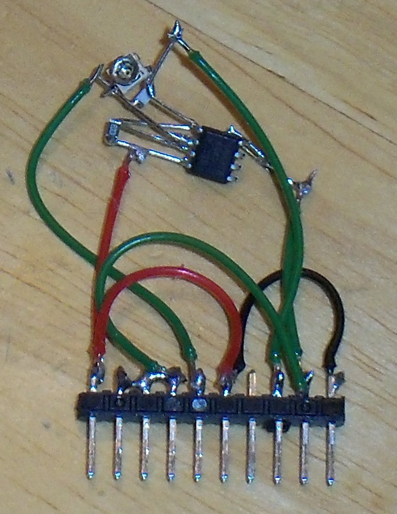
Here is the sleep mask with the infrared REM emitter/detectors installed; I've tried to keep as little as possible of the circuit installed on the mask.  The leads from the emitter and detectors (emitter in the middle) are folded over to keep them all in place.  The wires are sewn onto the mask to keep things tidy.  The longer  unconnected wires will eventually be trimmed and connected to a visible LED in each eyecup.

Finally, I've put together the first stage of the REM detector amplifier (shown below).  I've already had to reduce the value of the transimpedance feedback resistor from what had been used before to prevent output saturation.

Next steps

The immediate next step is to take a look at the output of the mocked-up amplifier to determine the characteristics of the REM reflectance signal.  My first priority is to nail down the ideal value of the transimpedance feedback resistor to allow for the largest gain without being unable to maintain the voltage between the phototransistors at 3.3V/2.  Additionally, this investigation should reveal what the effective bandwidth of the signal is, informing my choice of sampling rate.

After that, I will completely specify and prototype the whole REM detector circuit.  Specifically, I will try out the pulsed-emitter idea I had to reduce power consumption.  It will be necessary to see how long the rise time is for the output once the emitter is activated; also, I've got to make certain that the differential output current isn't affected (beyond the obvious) by being pulsed.

Soon after (and during) those steps, I'm going to mock up the power and programming and USB lines for the ATXMEGA controller, programming it with Atmel's USB-based bootloader to make subsequent reprogramming easier.  I'll also make sure that I can talk to the OLED display.

At that point, I think I'll be ready to design and purchase the boards.  I still won't have prototyped the LiPo charger and headphone amplifier circuits, but these are very straightforward (and adequately datasheet-ed) and shouldn't present any surprises.