Wednesday, May 22, 2013

How to export vector figures from MATLAB (or, the saddest thing is how elated I was when I finally figured this out)

Lately, I've been producing a lot of figures for my dissertation in MATLAB (my scientific computing platform of choice).  Once the figures are created, they need to be transferred into a word processor (e.g, Microsoft Word) to become part of my contribution to the advancement of science.

The problem is that this is a more complicated procedure than one might think.  The most straightforward method would be to save the figures as some sort of bitmap format (png, jpg, etc.); however, this means that the resolution is set and the figure labels, annotations, trace widths, etc. cannot be changed without going back to MATLAB, changing those things in the figure, then re-exporting it.  The alternative is to save the figure in a vector format; .eps would be ideal, but Word's support is spotty, so I use .emf.  A vector format saves a description of the shapes that make up the figure (lines, letters, patches of color) rather than a raster of pixels; this way, you can unpack the figure after-the-fact and change things in the word processor (line widths, fonts, labels) without having to go back to MATLAB.

The problem I had was that the vector images that MATLAB exported were... jagged.  Disjointed.  Weird.  Specifically, I need to plot EMG traces (ElectroMyoGrams, the electrical activity of muscles); some examples of this are shown immediately below.  The two figures immediately below are screenshots of the same data from within MATLAB; the left is just a zoomed-in subset of the right figure.  As you zoom in, MATLAB re-renders the image on the screen based on the actual data that was plotted.

Several traces of EMG, as seen natively in MATLAB
Zoom in of EMG traces, natively in MATLAB, showing normal spikiness of EMG
 The problem happened why I tried to export these figures into a vector format that I could insert into a Word document.  I first tried exporting as .eps; this did not work AT ALL.  When I exported to .emf, things appeared to work better (see the screenshot immediately below).  However, when zoomed in, the traces were 'jagged'.  Additionally, smoother traces (joint angles corresponding to the EMG) appeared 'quantized' far more than in the original figure.
Screenshot of exported figure in PowerPoint
Screenshot within Powerpoint of the figure above, zoomed in, showing 'jagged' trace
This was very confusing; why would the vectors be quantized? they represent the underlying data from the figure, right?  Searching online was largely in vain; the keyword 'jagged' was of no help, and most of what turned up was just generic 'how do I export MATLAB' how-tos.  After trying a series of progressively more esoteric and unnatural transformations (export to eps, open in ghostscript, export to emf, import into Powerpoint...), I finally found this thread on the MATLAB Central forum.  A few posts in, one person notes that "

 the resolution of the metafile is limited to screen resolution. This
means when we draw a line segment the endpoints are on a grid at screen
resolution. So even though the line is drawn at device resolution the
endpoints could be at a much lower resolution. This problem usually shows up
when you have lots of short line segments -- Ben Hinkle
AHA!  I had my answer.  The problem was not bad emf support in MATLAB or Powerpoint, but the fact that the default renderer creates the ends of the line segments in the vector image export at the resolution of the screen.  However, that post was from 2000, so MATLAB has advanced slightly since then; I was able to find an export setting that allowed me to force the resolution of the renderer to be higher than the screen resolution.

So, in the end, my MATLAB-to-Word (by way of Powerpoint for manipulation, because I am too cheap for Corel et. al) is:


  1. Create the figure in MATLAB
  2. In the MATLAB figure window, File -> Export Setup; under the Rendering tab, choose 'Painters' as the renderer (the other two are rasterizers) and 600 as your DPI (or 300 or 100, whatever floats your boat).  Presumably, 'Auto', which it was set to, had somewhat too-low standards for my needs.
  3. Apply to Figure
  4. Export -> set your file type as .emf.
  5. In Powerpoint, Insert -> Picture -> choose your figure
  6. Right click on the figure -> ungroup -> yes (this 'unpacks' the figure in Powerpoint, allowing you to manipulate the vector objects that make it up)
  7. Manipulate the figure, then directly copy/paste into Word (don't forget to re-group the figure elements before copying)

The end result is seen below; unfortunately, Powerpoint wouldn't let me zoom in any further, but it's clear that the figure as exported is far more faithful to the original than before the 600DPI setting.  Additionally, smoother traces no longer suffer from 'quantization'.


Thursday, March 7, 2013

Toward triangular-tesselated Game of Life wrapped onto regular polyhedra (or, MATLAB's handle graphics interface is simultaneously terrible and the best solution possible)

As I outlined in a previous post, I want to build a device which will display Conway's Game of Life.  To make things a little more interesting, it will do this using a triangular tesselation (rather than the much more common square pattern), and faces of 25 pixels will be folded and assembled to form a regular polyhedron.

Since building the device will be a large undertaking and the firmware will be very complicated (in a way which would make small errors generally difficult to isolate), I have implemented the device in simulation using the MATLAB environment.  This has allowed me to verify that my mapping of the pixels and implementation of the game update rules is correct.

Tetrahedron

The first shape is the tetrahedron, show below.  Since the tetrahedron is difficult to visualize in a 2D projection, I've posted two images of the same pattern from two different angles.  It's a period-3 oscillator under the rule {4,6,4,4}.  Implementing this form will only require one of the four-triangle circuit sets I've designed.

Octahedron

Below, I show show the evolution of a glider pattern, also under rule {4,6,4,4}.  The period of its circumnavigation of the device is 45.


Icosahedron

The same glider pattern, also rule {4,6,4,4}.  Circumnavigation takes 75 generations.


Source

The MATLAB files I used are here.  To instantiate one of the above forms, just run createIcosaTRI([4,6,4,4]), with your desired rule in the brackets.  The other shape creation functions are createTetraTRI and createOctaTRI.

Saturday, February 23, 2013

Initial validation of joint sensor glove board (or, at least I didn't put the USB jack in backwards this time)

As I related in a past post, I recently designed and built a device which could be built into a joint-sensor glove; it is able to measure the resistance of 25 sensors and store that data to a microSD card or stream it over a serial link.

I started this project because I've long wanted to play around with using an instrumented glove which would allow free-form hand gestures to be used as a human interface.  Additionally, I work with people who do research into physical rehab, who sometimes need access to hand movement data.  Currently, they have to use a bulky device which is wirelessly tethered to a PC; this restricts the circumstances under which data can be taken.  This device, being able to be contained in a glove and being able to store data internally, may allow for experiments which are not currently viable (e.g., a full-day recording to examine the structure of normal hand use).

Hardware

A front image of the board is below.  The front only has two buttons, two status LEDs, and the low-frequency, high-accuracy clock oscillator.


The back of the board is below.  The resistive sensors would be connected to the header at the top; the top row of holes all connect to +3.3V and the bottom row lead to the FET switch array.  Currently, I've got a potentiometer connected for first-round debugging.

The actual resistance-sensing circuitry uses a FET and an opamp to sink a set amount of current through the selected sensor channel.  The sensor channel is selected by turning ON the appropriate FETs in the line of ICs just below the sensor header at the top; it is a 5-by-5 array, allowing one of 25 sensors to be selected by the appropriate use of 10 outputs.  The voltage at the bottom of this switch array is sampled to measure the resistance; since the current sink is controlled, the voltage difference between 3.3V and the measured voltage determines the resistance.

The board also includes the microSD slot (bottom left) and the power circuitry (charger and 3.3V buck converter, bottom right).  All of the circuitry has been tested except the microSD slot.


Software + Testing

To start testing the hardware, I developed a simple firmware which will sample the 25 sensors and transmit the resulting voltages over the serial channel that I have broken out for debugging.  The firmware source is here; it is very simple, and applies a constant sink current across all of the sensors and over time.  In the future, it may make sense to adjust the sink current to match the sensitivity and range of the device to the magnitude and range of resistances exhibited by each channel.

The firmware sets the switch array and samples each 'sensor' in turn; the data is then partitioned and inserted into a transmit buffer.  Once all of the channels have been sampled, I use the DMA controller to 'automatically' transmit the buffer contents over the serial link.

To watch the data as it comes in, I use an upgraded version of my general-purpose MATLAB serial data 'scope function (here).  First, I verified that all of the channels were working by shorting each channel in turn (shown below); as you can see, all of the channels were working.


I then wiggled the potentiometer at either end of its range, to cause wiggles in the scope for the appropriate channels (below).


This means that, with the exception of the SD card slot, all of the hardware has been tested and verified.

Moving Forward

Since I know that the resistance sensor circuit works (in a broad sense), there are a number of things to do:

-Implement the SD-card logging.  This will involve testing out the hardware and its ability to interface with SD cards, looking up the specs for SD card partitioning and FAT32, and using that information to implement some simple code that finds a long stretch of unused space on the card to fill up with logged sensor data.  It would be possible to code something that does not require a contiguous segment of the drive; however, this would require a much more complicated algorithm.  Since this is a very purpose-built device, that seems like overkill; one merely needs to make sure that the SD cards used are relatively empty and absolutely defragmented.

-Implement a limited USB serial port.  At present, the hardware is able to communicate over USB (verified by flashing the device with a USB-based bootloader).  However, I do not use this facility; further, to get debug or other data out of my prototypes, I use a separate USB-to-serial cable connected to a debug USART.  This extra cable is somewhat cumbersome; it would be nice to only need to plug in one cable to power the device and allow for debugging and reprogramming.

-Make an example resistive joint sensor; develop the algorithms to read it.  At present, I just set the sensor current sink to a constant level.  However, for certain ranges of resistances to-be-measured, it will saturate, while others will barely register.  Additionally, an increase in resolution may be possible by sampling the sensor output single-ended, then also sampling it differentially with a bias input set equal-ish to the single-ended value.

-Make a glove; fill it with joint sensors.  Obviously, I eventually need to actually make a glove to sew sensors into, and then connect to the device.

Migration to sleep mask v2 (or, the device now lacerates the user's face in only 12% of use cases)

So, I finally got the hardware for the second version of the sleep mask to work.  Turns out, if your firmware waits for the real-time clock to stabilize the external crystal oscillator, it helps to have one attached.

The device front and back are pictured below; it is running on its own power, and all of the main subsystems are working.


Of course, I forgot to add a line from the battery to the ADC to allow for charge status to be monitored; that's one definite change for V3.

Moving forward, I need to:

-Take a few nights' worth of data, to make sure that the REM detector still works
-Develop a filter/classifier to determine whether REM was happening based on the detector output.
-Assess power usage again, and implement the lowpass in front of the headphone amplifier to see if that reduces power use.
-See what's going on with the headphone detection circuit; I cribbed this from an application note, and it was implied that it would just give a digital output; this has not been the case.

After the classifier is determined, I'll start to design the overall structure of the working firmware; it'll have to take into account the needs of the REM classifier and the headphone noise generator while also keeping track of current time, alarms and current and past REM states.


Friday, February 22, 2013

First steps for unnecessarily complicated paperweight (or, inconsequential blinking-light projects evolved)

For a long time, I've wanted to make a project that implemented Conway's Game of Life in electronics, as a kind of creating-for-its-own-sake thing.  The Game of Life (GoL) is a program that computes the 'evolution' of a population of cells on a square, 2-D plane.  It has some interesting computational properties, but I was mostly interested in it because, when observed over time, the cells have a kind of ordered chaos aesthetic.

My original yen (more than a decade ago) was to just build a HUGE matrix of LEDs and use them to display  the ongoing evolution via GoL of a random starting seed state.  However, this is A) expensive, in both space and currency; and B) not novel any more.  There have been a number of physical GoL implementations; in fact, you can buy a kit for a four-by-four matrix which can be tiled with other kits to make an arbitrarily large GoL implementation.

Playing around with the idea, I recently decided to make something out of the GoL with a triangular tessellation, rather then the usual square grid.  Fortunately, there was some literature on this subject (Bays, Carter. Cellular Automata in the Triangular Tesselation. Complex Systems 8 (1994) 127-150), so I didn't have to reinvent the wheel; additionally, his work specified which GoL rules would lead to interesting behavior.  He also discovered several glider patterns, so that I could incorporate them into non-random, pre-specified seed states if I so wanted.

I made a quick-and-dirty triangular tessellation display, as seen in the video below; I hooked it up to an ATXMEGA32A4U with a firmware that would start with a pattern, then allow it to evolve over time until there are no cells left, at which point it would reset to the original test state.


My goal was to create independent 5-by-5 triangular units which could be used as the faces of an icosahedron.  However, this ended up requiring a LOT of microcontrollers and a LOT of by-hand jumper soldering, owing to difficulties in routing one tiny board with a big microcontroller on one side.  I've since settled on a design which uses one microcontroller per four faces; this made the routing easier (in only have to solder the edges of the triangles together, with on jumpers) and significantly reduced the overall project cost, since I would only need five microcontrollers instead of 20.

At present, I have the set of boards for the matched four triangular faces designed, and the bill of materials for the faces set.  I just need to double-check those boards, design the power supply circuitry for the center of the icosahedron, add a board for V2 of the turn signal gloves, finish my doctoral thesis, sit for the USPTO registration examination and start my new job.  i expect to resume work on this project sometime after Labor Day.  2014.

Sunday, December 16, 2012

Replacing the middle button on the Logitech M570 Wireless Trackball (or, yes, I really do love this trackball that much)

I've been using a wireless trackball for a while now, and it's turned out to be one of the best purchases I've ever made.  It's especially excellent for working on the train, since i don't like the trackpad and there isn't room for a normal mouse.

The wireless trackball I'm using is the Logitech M570.  It has a combination scroll wheel/middle button; however, over time this button began to get flaky.  There would be weeks where the button wouldn't respond at all, or would only respond to exceptional force. Looking online, this seems to be a common problem; the device is somewhat cheaply made, and the middle button is not the usual high-performance switch, but some lower-quality part.

I set out to determine whether the button could be replaced; I was successful, and my procedure for replacing it is outlined below.  The new button is slightly stiffer than the old, but it works consistently.

Button Replacement Procedure

Disassembly

First, pop the blue trackball out.  Then, there are five screws holding the shell together; remove them.  Note that one of these screws is beneath the sticker in the battery compartment (shown below).


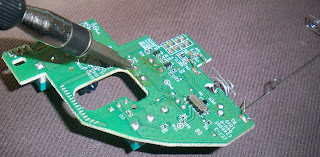
With the shell off, you'll need to remove the circuit boards.  First, detach the ribbon cable leading to the trackball reader (the gold bit in the middle of the image below); to do this, you'll have to pull up the plastic locking connector.  Then, remove the four screws which keep the circuit boards on the lower shell, and pick up the circuit board assembly.  Take care not to bend the battery wires as you remove them from the lower shell.  The middle/scroll wheel button we're going to replace is just in front of the ribbon cable.


Old Button Removal

In removing the old button, we need to be careful not to damage the rest of the circuitry.  Note that our task is made easier by the fact that we don't care what state the old button ends up in.  The method I used to avoid damage to the surrounding circuit is shown below; first, I used a diagonal cutter to cut the two forward leads on the button.  Once this was done, I gently rocked the button up and down to weaken and then break the remaining two leads of the button and remove it (I did not cut these leads, as there were difficult to access without risking damage to the rest of the circuit).


Once the button is mostly removed, I used copper solder wick to clean up the four holes that the leads of the button formerly inhabited.

New Button modification and installation

If you were paying close attention during the old button removal, you'll notice that the leads were pretty much vertical.  The buttons I had on hand were very similar in size and function (normally open, leads paired length-wise); however, their leads were gull-wing SMD style (MOUSER link).  Before I can install it, I need to manipulate the leads into a more vertical configuration, detailed in pictures below.


First, push the leads down.


Then, use pliers to straighten the leads downward.


Then, gently insert the button into the cleared holes and solder it into place; be sure that it is flush with the surface of the circuit board.


Re-Assembly

Just reverse the steps in Disassembly.  It is important to make sure that the little plastic power button in the lower shell is lined up with the switch on the circuit board before screwing everything back together (the switch is the silver-and-black affair on the lower right of the picture above, just in front of where the battery clips attach to the circuit board).


It is interesting to note that Logitech uses Nordic Semiconductor radios for their wireless links (at least for the new-ish unified receiver).

Tuesday, December 11, 2012

My initial investigation of the MARLOK key (or, how many times do I have to mess up using a pipelined ADC before I'll learn my lesson permanently?)

As I mentioned in the previous post, my university uses a somewhat rare access control technology called 'MARLOK': each user is issued a key, whose identity is encoded in a series of holes in the shank of the key (kind of like an old punch-card).  The key is inserted into a reader next to a door, and if the user has privileges to the door, it is momentarily unlocked.

I was interested in reading the key (and possibly eventually building something to emulate the key, in a reader), so I had a couple of little boards made to mount infrared emitters and detectors at the appropriate distances to read the three tracks of the key.

Initial Research

Before doing all this, I tried to look up the MARLOK system on the internet.  Details were sparse; the only information of any substance is here, where someone reports that each key encodes 24 bits of ID.  Otherwise, there's very little info out there; nothing on the structure of the encoding, how the clock is embedded/recovered, etc.

The Current Test

The sensor (with key inserted) is shown below.  The emitters are Kignbright APT2012F3C; they are wired in parallel with a 460Ohm current limiting resistor, leading to a total of 5mA passing through them collectively.  The detectors are Everlight PT19-21C/L41/TR8 phototransistors; they are connected to the positive rail, and then through 2.2kOhm resistors to ground.  The voltage is sampled at the top of the resistors by a microcontroller, then sent out at 100Hz through the serial port.

The key has three tracks; the black plastic is infrared-transparent.  The metal of the key is punched with square holes to allow for IR light to travel through the key.


The ends of two of the tracks were totally accidentally exposed, to show the structure of the holes (shown below).  As you can see, the holes are square.  From the data I show later, the middle track is a clock signal; this makes sense, as the middle hole is offset from the exposed side track by a half-hole-width, so that transition on the clock track signals when to sample the data tracks.


Below is a plot of the three track traces; the left is when the sensor was seated at the base of the key, and the right occurred as I slid the sensor off the key.  Green is the middle track, red and blue are the side tracks.  Note that it took a little messing around to get this data; originally, the LED current was three times what it was for these trials, and it saturated the clock channel (since, being in the middle, it got illumination from all three LEDs).


This next is the same information, but at the end of the sensor removal, as the sensor comes of the end of the key.


From the data, I saw that the middle track was the only one that was always on; from this (and the fact that its holes were offset from the other tracks' holes), I assume it is the clock signal.

Looking at the traces over a full sensor-removal, I saw the following patterns of holes:

01111110011101
11111111111111 END OF KEY>>
00001001110111
As i said above, the middle track was the only one that was always 'on'.  Additionally, since the first clock has both 'on', and the last has both 'off', and the internet says these keys encode 24 bits, and there are 14 total clock pulses, I assume that the end-of-key data track bits are always 'on', and the base-of-key data track bits are always 'off', which likely helps in level determination and data recovery.

Moving Forward

As evidenced in the data traces, I'm having difficulty keeping the key straight in the sensor; I'll need to do something to mechanically narrow the passage.  Once this is done, it'll be possible to recover sampling times from the clock transitions.  It might also be possible to improve the signal level by masking the LEDs so that they don't bleed over into the other channels as much.

Data Recording Software

To get this data, I created a microcontroller firmware that samples the three channels, then packs each 12bit sample into a message packet (which includes a start sentinel nibble for frame alignment) and sends it over the serial port.  I then created a general-purpose serial port data-extractor and -viewer for MATLAB, which is available here.